Revisions and Notes
Date | Owner | Revision | Notes | ||||||||
| Rabeeh Khoury | 1.0 | |||||||||
Table of Contents |
| ||||||||||
| Info |
|---|
No warranty of accuracy is given concerning the contents of the information contained in this publication. To the extent permitted by law no liability (including liability to any person by reason of negligence) will be accepted by SolidRun Ltd., its subsidiaries or employees for any direct or indirect loss or damage caused by omissions from or inaccuracies in this document. SolidRun Ltd. reserves the right to change details in this publication without prior notice. Product and company names herein may be the trademarks of their respective owners. |
Introduction
This document is intended for hardware engineers that are willing to integrate
LX2160A COM express type 7 module from SolidRun ltd.
The document provides details with regards LX2160A module rev 1.3, 1.4, 1.5 and 1.6.
Specifications
Form Factor | COM Express type 7 | ||||||||
Processor Core | 16 core Arm Cortex A72 | ||||||||
Processor speed | Up to 2GHz | ||||||||
Memory | Dual channel SO-DIMM DDR4; up to 64GB 3200MT/s (not included by default)* | ||||||||
ECC | Optional | ||||||||
eMMC | 64GB by default (up to 128GB) | ||||||||
SATA | 2 x SATA (Gen III)** | ||||||||
Security | NXP LX2160A Secure Boot | ||||||||
Supported OS | Linux kernel 4.14x | ||||||||
XFI/RXAUI/SGMII | 4** | ||||||||
PCIe gen 3.0 | 18 (5 controllers)** | ||||||||
SGMII | 1 with built in phy | ||||||||
USB 3.0 | 4 | ||||||||
I2C | 6 | ||||||||
UART | 2 | ||||||||
SPI bus | ✓ | ||||||||
Power | 12V (9V-15V) | ||||||||
Environment | Commercial: 0°C to 70°C | ||||||||
Dimensions | 125mm X 95mm | ||||||||
|
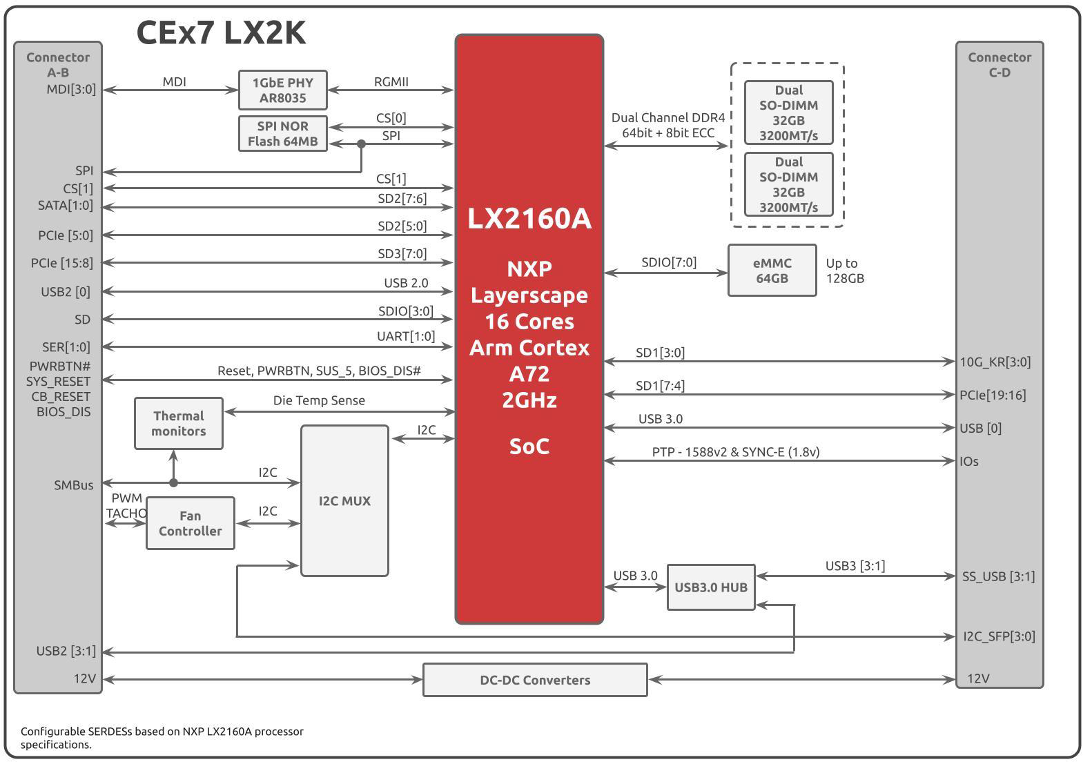
Overview
LX2160A COM express type 7 is a highly integrated COM modules based on NXP’s LX2160A SoC.
The SoC highlights are up to 2.0GHz 16 x Cortex A72 Arm cores, two DDR4 controllers up to 3200Mtps and 24 high speed SERDESes.
The module integrates the following features –
LX2160A SoC (up to 2.0GHz).
Two SO-DIMM DDR4 connected to the two DDR contorllers. Each SO-DIMM supports up to 32GByte SO-DIMM DDR4 3200Mtps memory with and without ECC, registered or non-registered; total up to 64GByte system memory.
Single 12v DC-input is required.
Description
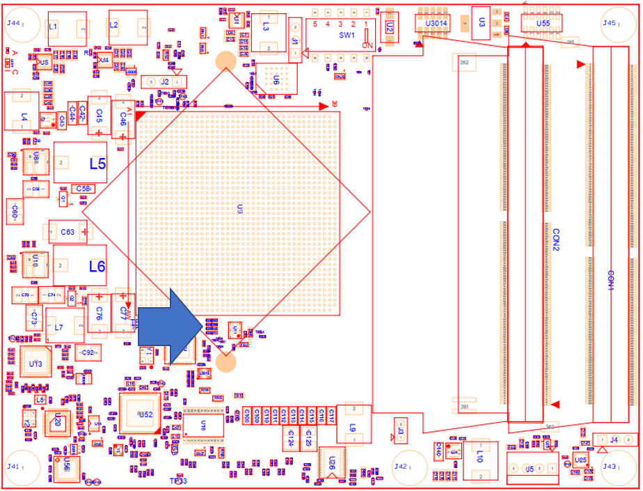
Block Diagram
The following figure describes the LX2160A COM express type 7 Blocks Diagram.
Simplified Schematics
Following is a link to that simplified schematics of the board : LX2160A COM Simplified Schematics
LX2160A COM express type 7 simplified schematics is intended for the following audience –
Software and firmware engineers that enables them to understand the IO and signal connectivity of the COM express design.
Hardware engineers that are willing to use the COM express and build their own development board. This document completes the CEx7 LX2160A reference manual from description of signal and implementation wise.
S-Parameters
Browse below in the Documentation section in other files section to download LX2160A-CEX7 S-parameters.
The 25 GbE files refer to the 10G KR signals – total 32 ports model up to 20GHz and the second PCIe file refers to all other SERDESes while the model is up to 6GHz.
Module Power Consumption Measurements
The following power consumption measurements were conducted on the following setup –
HoneyComb LX2 mini-ITX motherboard with pico-psu ATX power source
LX2160A COM express type 7 module connected running at 2GHz core, 700 MHz fabric and 3200Mtps DDR
Two SO-DIMM DDR4 at 3200Mtps (total 2x8GB = 16GByte system memory)
During the tests an 1.3Watt fan mounted on the processor. The idle, memtester and first cpu-burn power measurements below includes those 1.3Watt, the measurements with die temperature of 65c and above has the fan disconnected.
Temperature measurement was done using Linux ‘sensors’ commands, that reads both the PCB (print side of the board away from the center) and the processor die temperature.
Software running is based on NXP LSDK-19.06 software release.
A 12v PSU is connected to a pico-psu (12v to ATX); and power is measured by multiplying the current and the voltage on the 12v input rail.
Since the measurement is done on the input of the pico-psu; the SoC consumption all together with the DDR and all the DC-DC losses are measured too.
Test | Power (Watt) | PCB Temperature (Celsius) | Die Temperature (Celsius) |
Linux idle | 21.5 | 40 | 44.6 |
16x memtester 100M (*) | 36.5 | 48 | 56.9 |
2x cpuburn-krait (**) | 35.6 | 48.4 | 59.1 |
2x cpuburn-krait (***) – no fan | 40.1 | 78.8 | 105 |
| Note |
|---|
Please note (*) – The Linux command is ‘memtester 100M > /dev/null &’ ran 16x times where 16 is the core count (**) – The Linux command ‘cpuburn-krait’ is ran two times in background. The reason cpuburn-krait was chosen since it can generate most heat out of the cores (the core pipeline most utilized). (***) – This measurement was taken when the fan is disconnected and the power was measured when the die reached 105c. Notice that keeping the fan disconnected will make the processor reach temperatures that are out of spec. |
Maximum Current Consumption
The LX2160A type 7 uses only the 12v power rail to supply it’s internal components.
The user of this module must make sure that the 12v power rail provided to the COM can sustain 5A, i.e. total 60W.
Notice the above section on power measurement using memtester and cpuburn applications which is worst case scenario of ~40@ when the core junction is at 105c; taking into account different SO-DIMMs used and variance in processor leakage due to silicon manufacturing environments, we recommend to design the carrier board to sustain those 5A on the 12V rail.
PCIe Lane Numbers and Bucket Grouping
Following is the bucket grouping of the different PCIe lanes.
Bucket B1 – lanes #0 .. #7
There is a single configuration in this bucket –
x4 PCIe lanes 0,1,2,3 connected to controller #3 (SERDES SD2 lanes 0,1,2,3)
x2 PCIe lanes 4,5 connected to controller #4 (SERDES SD2 lanes 4,5)
PCIe lanes 6,7 are NC
Notice that it is possible to gang PCIe lanes 0..5 with SATA0 and SATA1 and which makes all SD2 lanes 0..7 and have a single x8 gen3 controller #3. In this configuration the on COM module DC bias serial capacitors are required to be changed to 220nF instead of 10nF (contact SolidRun for more information)
Bucket B2 – lanes #8 .. #15
There are two possible configurations in this bucket –
2 times x4 – Lanes 8 to 11 connected to controller #5 and lanes 12 to 15 connected to controller #6.
1 time x8 -Lanes 8 to 15 are connected to controller #5
Bucket B3 – lanes #16 .. #23
There is a single configuration in this bucket –
Up to 1 time x4 – lanes 16 .. 19 on controller #2.
Lanes 20 to 23 are NC.
Notice that this configuration highly depends on the SD1 SERDES protocol number configuration. Please follow SD1 protocol number configuration in this document that explains how those lanes are affected.
Bucket B4 – lanes #24 .. #31
All lanes in this bucket are NC.
SERDES configuration
LX2160A has 3 SERDES blocks named SD1, SD2 and SD3.
SERDES block #1 (SD1)
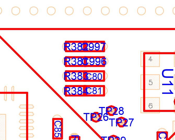
SERDES block #1 (SD1) has the most different options to configure from. By default the board is assembled with PLLF=161.1328125MHz and PLLS=100MHz, spread spectrum disabled.
In order to modify swap both PLLF and PLLS to be 100MHz:
Remove Move C996 , and C997 , to C80 , C81 Assemble 0R resistor at R381, R382, R383, R384and C81 (same value 100nF low ESL 0402 capacitor). This will move the 161.1328125MHz from PLLF to PLLS
Move R383 and R384 to R2381 and R382 (zero ohm 0402 resistors). This will move the 100MHz reference clock from PLLS to PLLF
** these capacitors/resistors have shared pads as shown in the picture below
Each SERDES block has 8 SERDESes that can be configured by protocol number.
Noticve: The Default clock assembly limits the amount of configurations according to the table below:
Protocol | Lane 0 10G-KR0 | Lane 1 10G- KR1 | Lane 2 10G-KR2 | Lane 3 10G-KR3 | Lane 4 PCIe16 | Lane 5 PCIe17 | Lane 6 PCIe18 | Lane 7 PCIe19 | Notes |
0 | off | off | off | off | off | off | off | off | |
1 | PCIe.1 x4 | PCIe.2 x4 | (*) | ||||||
2 | SGMII.3 | SGMII.4 | SGMII.5 | SGMII.6 | PCIe.2 x4 | (*) | |||
7 | XFI.3 | XFI.4 | |||||||
AB Header
Notes | Driving IC | Schematics Pin Name | Pin Number | Pin Number | Schematics Pin Name | Driving IC | Notes | |
|---|---|---|---|---|---|---|---|---|
| 1 | GND (FIXED) | A1 | B1 | GND (FIXED) | ||||
| 2 | AR8035 | GBE0_MDI3- | A2 | B2 | GBE0_ACT# | AR8035 LED_ACT | ||
| 3 | AR8035 | GBE0_MDI3+ | A3 | B3 |
| |||
| 4 | Not used |
| A4 | B4 |
| |||
| 5 | AR8035 LED_1000 pin 22 | GBE0_LINK1000# | A5 | B5 |
| |||
| 6 | AR8035 | GBE0_MDI2- | A6 | B6 |
| |||
| 7 | AR8035 | GBE0_MDI2+ | A7 | B7 |
| |||
| 8 | AR8035 LED_10_100 pin 24 | GBE0_LINK# | A8 | B8 |
| |||
| 9 | AR8035 | GBE0_MDI1- | A9 | B9 |
| |||
| 10 | AR8035 | GBE0_MDI1+ | A10 | B10 |
| |||
| 11 | GND (FIXED) | A11 | B11 | GND (FIXED) | ||||
| 12 | AR8035 | GBE0_MDI0- | A12 | B12 | PWRBTN# | 3.3v, GPIO3[6], 2.2k pull-up | ||
| 13 | AR8035 | GBE0_MDI0+ | A13 | B13 | SMB_CK | I2C1 - CH#3 | ||
| 14 | Not used |
| A14 | B14 | SMB_DAT | I2C1 - CH#3 | ||
| 15 |
| A15 | B15 | SMB_ALERT# | 3.3v, EVT0, GPIO3[12], 2.2k pull-up | |||
| 16 | Serial 10nF | LX2160A SD2 SRDS6 | SATA0_TX+ | A16 | B16 | SATA1_TX+ | LX2160A SD2 SRDS7 | Serial 10nF |
| 17 | Serial 10nF | LX2160A SD2 SRDS6 | SATA0_TX | A17 | B17 | SATA1_TX | LX2160A SD2 SRDS7 | Serial 10nF |
| 18 |
| A18 | B18 |
| ||||
| 19 | Serial 10nF | LX2160A SD2 SRDS6 | SATA0_RX+ | A19 | B19 | SATA1_RX+ | LX2160A SD2 SRDS7 | Serial 10nF |
| 20 | Serial 10nF | LX2160A SD2 SRDS6 | SATA0_RX | A20 | B20 | SATA1_RX | LX2160A SD2 SRDS7 | Serial 10nF |
| 21 | GND (FIXED) | A21 | B21 | GND (FIXED) | ||||
| 22 | Serial 220nF | LX2160A SD3 SRDS7 | PCIE_TX15+ | A22 | B22 | PCIE_RX15+ | LX2160A SD3 SRDS7 | |
| 23 | Serial 220nF | LX2160A SD3 SRDS7 | PCIE_TX15- | A23 | B23 | PCIE_RX15- | LX2160A SD3 SRDS7 | |
| 24 | 3.3v, GPIO3[7], 2.2k pull-up | SUS_S5# | A24 | B24 | PWR_OK | Power management IC | Refer to power-up sequence | |
| 25 | Serial 220nF | LX2160A SD3 SRDS6 | PCIE_TX14+ | A25 | B25 | PCIE_RX14+ | LX2160A SD3 SRDS6 | |
| 26 | Serial 220nF | LX2160A SD3 SRDS6 | PCIE_TX14- | A26 | B26 | PCIE_RX14+ | LX2160A SD3 SRDS6 | |
| 27 | 3.3v, EVT4, GPIO3[16], 2.2k pull-up | BATLOW# | A27 | B27 |
| |||
| 28 |
| A28 | B28 | RSVD | ||||
| 29 | RSVD | A29 | B29 | RSVD | ||||
| 30 | RSVD | A30 | B30 | RSVD | ||||
| 31 | GND (FIXED) | A31 | B31 | GND (FIXED) | ||||
| 32 | RSVD | A32 | B32 |
| ||||
| 33 | RSVD | A33 | B33 | I2C_CK | LX2160A I2C2 | |||
| 34 | SPI CS0/1 switch, 3.3v, 2.2k pull-up | BIOS_DIS0# | A34 | B34 | I2C_DAT | LX2160A I2C2 | ||
| 35 |
| A35 | B35 | THRM# | 3.3v, EVT1, GPIO3[13], 2.2k pull-up | |||
| 36 | Serial 220nF | LX2160A SD3 SRDS5 | PCIE_TX13+ | A36 | B36 | PCIE_RX13+ | LX2160A SD3 SRDS5 | |
| 37 | Serial 220nF | LX2160A SD3 SRDS5 | PCIE_TX13- | A37 | B37 | PCIE_RX13- | LX2160A SD3 SRDS5 | |
| 38 | GND | A38 | B38 | GND | ||||
| 39 | Serial 220nF | LX2160A SD3 SRDS4 | PCIE_TX12+ | A39 | B39 | PCIE_RX12+ | LX2160A SD3 SRDS4 | |
| 40 | Serial 220nF | LX2160A SD3 SRDS4 | PCIE_TX12- | A40 | B40 | PCIE_RX12+ | LX2160A SD3 SRDS4 | |
| 41 | GND (FIXED) | A41 | B41 | GND (FIXED) | ||||
| 42 | USB3.0 HUB port 2 | USB2- | A42 | B42 | USB3- | USB3.0 HUB port 3 | ||
| 43 | USB3.0 HUB port 2 | USB2+ | A43 | B43 | USB3+ | USB3.0 HUB port 3 | ||
| 44 |
| A44 | B44 |
| ||||
| 45 | LX2160A USB0 | USB0- | A45 | B45 | USB1- | USB3.0 HUB port 1 | ||
| 46 | LX2160A USB0 | USB0+ | A46 | B46 | USB1+ | USB3.0 HUB port 1 | ||
| 47 | 100nF and 22uF on module | PCF2129AT | VCC_RTC | A47 | B47 |
| ||
| 48 | RSVD | A48 | B48 | RSVD | ||||
| 49 | LX2160A TRIG_IN1 - Only rev 1.6 and newer. 1.8v signal | RSVD | A49 | B49 | SYS_RESET# | 3.3v, 2.2k pull-up, sys reset input | ||
| 50 |
| A50 | B50 | CB_RESET# | 3.3v, carrier board reset output (1uF capacitance) | |||
| 51 | GND (FIXED) | A51 | B51 | GND (FIXED) | ||||
| 52 | Serial 220nF | LX2160A SD2 SRDS5 | PCIE_TX5+ | A52 | B52 | PCIE_RX5+ | LX2160A SD2 SRDS5 | |
| 53 | Serial 220nF | LX2160A SD2 SRDS5 | PCIE_TX5- | A53 | B53 | PCIE_RX5- | LX2160A SD2 SRDS5 | |
| 54 | micro SD D0 | GPI0 | A54 | B54 | GPO1 | micro SD CMD | ||
| 55 | Serial 220nF | LX2160A SD2 SRDS4 | PCIE_TX4+ | A55 | B55 | PCIE_RX4+ | LX2160A SD2 SRDS4 | |
| 56 | Serial 220nF | LX2160A SD2 SRDS4 | PCIE_TX4- | A56 | B56 | PCIE_RX4- | LX2160A SD2 SRDS4 | |
| 57 | GND | A57 | B57 | GPO2 | 3.3v, GPIO3[5], 2.2k pull-up | |||
| 58 | Serial 220nF | LX2160A SD2 SRDS3 | PCIE_TX3+ | A58 | B58 | PCIE_RX3+ | LX2160A SD2 SRDS3 | |
| 59 | Serial 220nF | LX2160A SD2 SRDS3 | PCIE_TX3- | A59 | B59 | PCIE_RX3- | LX2160A SD2 SRDS3 | |
| 60 | GND (FIXED) | A60 | B60 | GND (FIXED) | ||||
| 61 | Serial 220nF | LX2160A SD2 SRDS2 | PCIE_TX2+ | A61 | B61 | PCIE_RX2+ | LX2160A SD2 SRDS2 | |
| 62 | Serial 220nF | LX2160A SD2 SRDS2 | PCIE_TX2- | A62 | B62 | PCIE_RX2- | LX2160A SD2 SRDS2 | |
| 63 | micro SD D1 | GPI1 | A63 | B63 | GPO3/SD_CD | micro SD CD (2.2k 3.3v pulled-up) | ||
| 64 | Serial 220nF | LX2160A SD2 SRDS1 | PCIE_TX1+ | A64 | B64 | PCIE_RX1+ | LX2160A SD2 SRDS1 | |
| 65 | Serial 220nF | LX2160A SD2 SRDS1 | PCIE_TX1- | A65 | B65 | PCIE_RX1- | LX2160A SD2 SRDS1 | |
| 66 | GND | A66 | B66 |
| ||||
| 67 | micro SD D2 | GPI2 | A67 | B67 |
| |||
| 68 | Serial 220nF | LX2160A SD2 SRDS0 | PCIE_TX0+ | A68 | B68 | PCIE_RX0+ | LX2160A SD2 SRDS0 | |
| 69 | Serial 220nF | LX2160A SD2 SRDS0 | PCIE_TX0- | A69 | B69 | PCIE_RX0- | LX2160A SD2 SRDS0 | |
| 70 | GND (FIXED) | A70 | B70 | GND (FIXED) | ||||
| 71 | Serial 220nF | LX2160A SD3 SRDS0 | PCIE_TX8+ | A71 | B71 | PCIE_RX8+ | LX2160A SD3 SRDS0 | |
| 72 | Serial 220nF | LX2160A SD3 SRDS0 | PCIE_TX8- | A72 | B72 | PCIE_RX8- | LX2160A SD3 SRDS0 | |
| 73 | GND | A73 | B73 | GND | ||||
| 74 | Serial 220nF | LX2160A SD3 SRDS1 | PCIE_TX9+ | A74 | B74 | PCIE_RX9+ | LX2160A SD3 SRDS1 | |
| 75 | Serial 220nF | LX2160A SD3 SRDS1 | PCIE_TX9- | A75 | B75 | PCIE_RX9- | LX2160A SD3 SRDS1 | |
| 76 | GND | A76 | B76 | GND | ||||
| 77 | Serial 220nF | LX2160A SD3 SRDS2 | PCIE_TX10+ | A77 | B77 | PCIE_RX10+ | LX2160A SD3 SRDS2 | |
| 78 | Serial 220nF | LX2160A SD3 SRDS2 | PCIE_TX10- | A78 | B78 | PCIE_RX10- | LX2160A SD3 SRDS2 | |
| 79 | GND | A79 | B79 | GND | ||||
| 80 | GND (FIXED) | A80 | B80 | GND (FIXED) | ||||
| 81 | Serial 220nF | LX2160A SD3 SRDS3 | PCIE_TX11+ | A81 | B81 | PCIE_RX11+ | LX2160A SD3 SRDS3 | |
| 82 | Serial 220nF | LX2160A SD3 SRDS3 | PCIE_TX11- | A82 | B82 | PCIE_RX11- | LX2160A SD3 SRDS3 | |
| 83 | GND | A83 | B83 | GND | ||||
| 84 |
| A84 | B84 |
| ||||
| 85 | micro SD D3 | GPI3 | A85 | B85 |
| |||
| 86 | RSVD | A86 | B86 |
| ||||
| 87 | RSVD | A87 | B87 |
| ||||
| 88 | HCSL PCIe Gen4 compliant | 100MHz clock gen | PCIE_CK_REF+ | A88 | B88 |
| ||
| 89 | HCSL PCIe Gen4 compliant | 100MHz clock gen | PCIE_CK_REF | A89 | B89 |
| ||
| 90 | GND (FIXED) | A90 | B90 | GND (FIXED) | ||||
| 91 | 3.3v power. gated by 12v input | SPI_POWER | A91 | B91 |
| |||
| 92 | 3.3v SPI MISO | SPI_MISO | A92 | B92 |
| |||
| 93 | micro SD CLK | GPO0 | A93 | B93 |
| |||
| 94 | 3.3v SPI CLK | SPI_CLK | A94 | B94 |
| |||
| 95 | 3.3v SPI MOSI | SPI_MOSI | A95 | B95 |
| |||
| 96 |
| A96 | B96 |
| ||||
| 97 |
| A97 | B97 | SPI_CS# | 3.3v SPI CS# | |||
| 98 | LX2160A UART1 (main) | SER0_TX | A98 | B98 |
| |||
| 99 | LX2160A UART1 (main) | SER0_RX | A99 | B99 |
| |||
| 100 | GND (FIXED) | A100 | B100 | GND (FIXED) | ||||
| 101 | LX2160A UART2 | CAN0/SER1_TX | A101 | B101 | FAN_PWMOUT | AMC6821 PWM-OUT (pin 1) | ||
| 102 | LX2160A UART2 | CAN0/SER1_RX | A102 | B102 | FAN_TACHIN | AMC6821 TACH (pin 2) through 3.3v level shifter | ||
| 103 |
| A103 | B103 |
| ||||
| 104 | 12v input (9v-15v) | VCC_12V | A104 | B104 | VCC_12V | 12v input (9v-15v) | ||
| 105 | 12v input (9v-15v) | VCC_12V | A105 | B105 | VCC_12V | 12v input (9v-15v) | ||
| 106 | 12v input (9v-15v) | VCC_12V | A106 | B106 | VCC_12V | 12v input (9v-15v) | ||
| 107 | 12v input (9v-15v) | VCC_12V | A107 | B107 | VCC_12V | 12v input (9v-15v) | ||
| 108 | 12v input (9v-15v) | VCC_12V | A108 | B108 | VCC_12V | 12v input (9v-15v) | ||
| 109 | 12v input (9v-15v) | VCC_12V | A109 | B109 | VCC_12V | 12v input (9v-15v) | ||
| 110 | GND (FIXED) | A110 | B110 | GND (FIXED) |
CD Header
Notes | Driving IC | Schematics Pin Name | Pin Number | Pin Number | Schematics Pin Name | Driving IC | Notes | |
|---|---|---|---|---|---|---|---|---|
| 1 | GND (FIXED) | C1 | D1 | GND (FIXED) | ||||
| 2 | GND | C2 | D2 | GND | ||||
| 3 | LX2160A USB0 | USB_SSRX0- | C3 | D3 | USB_SSTX0- | LX2160A USB0 | Serial 100nF | |
| 4 | LX2160A USB0 | USB_SSRX0+ | C4 | D4 | USB_SSTX0+ | LX2160A USB0 | Serial 100nF | |
| 5 | GND | C5 | D5 | GND | ||||
| 6 | USB3.0 HUB port 1 | USB_SSRX1- | C6 | D6 | USB_SSTX1- | USB3.0 HUB port 1 | Serial 100nF | |
| 7 | USB3.0 HUB port 1 | USB_SSRX1+ | C7 | D7 | USB_SSTX1+ | USB3.0 HUB port 1 | Serial 100nF | |
| 8 | GND | C8 | D8 | GND | ||||
| 9 | USB3.0 HUB port 2 | USB_SSRX2- | C9 | D9 | USB_SSTX2- | USB3.0 HUB port 2 | Serial 100nF | |
| 10 | USB3.0 HUB port 2 | USB_SSRX2+ | C10 | D10 | USB_SSTX2+ | USB3.0 HUB port 2 | Serial 100nF | |
| 11 | GND(FIXED) | C11 | D11 | GND (FIXED) | ||||
| 12 | USB3.0 HUB port 3 | USB_SSRX3- | C12 | D12 | USB_SSTX3- | USB3.0 HUB port 3 | Serial 100nF | |
| 13 | USB3.0 HUB port 3 | USB_SSRX3+ | C13 | D13 | USB_SSTX3+ | USB3.0 HUB port 3 | Serial 100nF | |
| 14 | GND | C14 | D14 | GND | ||||
| 15 | 3.3v 2.2k pull-up, shared with pin C45 | LX2160A MDC2 | 10G_PHY_MDC_SCL3 | C15 | D15 | 10G_PHY_MDIO_SDA3 | LX2160A MDIO2 | 3.3v 2.2k pull-up, shared with pin D45 |
| 16 | 3.3v 2.2k pull-up, shared with pin C46 | LX2160A MDC1 | 10G_PHY_MDC_SCL2 | C16 | D16 | 10G_PHY_MDIO_SDA2 | LX2160A MDIO1 | 3.3v 2.2k pull-up, shared with pin D46 |
| 17 | LX2160A - CLK_IN - Only rev 1.6 and newer. 1.8v signal | 10G_SDP2 | C17 | D17 | 10G_SDP3 | LX2160A - TRIG_IN2 - Only rev 1.6 and newer. 1.8v signal | ||
| 18 | GND | C18 | D18 | GND | ||||
| 19 |
| C19 | D19 |
| ||||
| 20 |
| C20 | D20 |
| ||||
| 21 | GND (FIXED) | C21 | D21 | GND (FIXED) | ||||
| 22 |
| C22 | D22 |
| ||||
| 23 |
| C23 | D23 |
| ||||
| 24 | LX2160A IRQ10 GPIO3[10] | 10G_INT2 | C24 | D24 | 10G_INT3 | LX2160A IRQ11 GPIO3[11] | ||
| 25 | GND | C25 | D25 | GND | ||||
| 26 | no DC blocking capacitors | LX2160A SD1 SRDS3 | 10G_KR_RX3+ | C26 | D26 | 10G_KR_TX3+ | LX2160A SD1 SRDS3 | no DC blocking capacitors |
| 27 | no DC blocking capacitors | LX2160A SD1 SRDS3 | 10G_KR_RX3- | C27 | D27 | 10G_KR_TX3- | LX2160A SD1 SRDS3 | no DC blocking capacitors |
| 28 | GND | C28 | D28 | GND | ||||
| 29 | no DC blocking capacitors | LX2160A SD1 SRDS2 | 10G_KR_RX2+ | C29 | D29 | 10G_KR_TX2+ | LX2160A SD1 SRDS2 | no DC blocking capacitors |
| 30 | no DC blocking capacitors | LX2160A SD1 SRDS2 | 10G_KR_RX2- | C30 | D30 | 10G_KR_TX2- | LX2160A SD1 SRDS2 | no DC blocking capacitors |
| 31 | GND (FIXED) | C31 | D31 | GND (FIXED) | ||||
| 32 | 10k pull-up | I2C1 CH7 | 10G_SFP_SDA3 | C32 | D32 | 10G_SFP_SCL3 | I2C1 CH7 | 10k pull-up |
| 33 | 10k pull-up | I2C1 CH6 | 10G_SFP_SDA2 | C33 | D33 | 10G_SFP_SCL2 | I2C1 CH6 | 10k pull-up |
| 34 | 3.3v, 2.2k pull-up | LX2160A EVT2 GPIO3[14] | 10G_PHY_RST_23 | C34 | D34 |
| ||
| 35 | 3.3v, 2.2k pull-up | LX2160A EVT3 GPIO3[15] | 10G_PHY_RST_01 | C35 | D35 |
| ||
| 36 | I2C1 CH3 | 10G_LED_SDA | C36 | D36 | RSVD | |||
| 37 | I2C1 CH3 | 10G_LED_SCL | C37 | D37 | RSVD | |||
| 38 | 10k pull-up | I2C1 CH5 | 10G_SFP_SDA1 | C38 | D38 | 10G_SFP_SCL1 | I2C1 CH5 | 10k pull-up |
| 39 | 10k pull-up | I2C1 CH4 | 10G_SFP_SDA0 | C39 | D39 | 10G_SFP_SCL0 | I2C1 CH4 | 10k pull-up |
| 40 | LX2160A PULSE_OUT1 - Only rev 1.6 and newer. 1.8v signal | 10G_SDP0 | C40 | D40 | 10G_SDP1 | LX2160A PULSE_OUT2 - Only rev 1.6 and newer. 1.8v signal | ||
| 41 | GND (FIXED) | C41 | D41 | GND (FIXED) | ||||
| 42 | no DC blocking capacitors | LX2160A SD1 SRDS1 | 10G_KR_RX1+ | C42 | D42 | 10G_KR_TX1+ | LX2160A SD1 SRDS1 | no DC blocking capacitors |
| 43 | no DC blocking capacitors | LX2160A SD1 SRDS1 | 10G_KR_RX1- | C43 | D43 | 10G_KR_TX1- | LX2160A SD1 SRDS1 | no DC blocking capacitors |
| 44 | GND | C44 | D44 | GND | ||||
| 45 | 3.3v 2.2k pull-up, shared with pin C15 | LX2160A MDC2 | 10G_PHY_MDC_SCL1 | C45 | D45 | 10G_PHY_MDIO_SDA1 | LX2160A MDIO2 | 3.3v 2.2k pull-up, shared with pin D15 |
| 46 | 3.3v 2.2k pull-up, shared with pin C16 | LX2160A MDC1 | 10G_PHY_MDC_SCL0 | C46 | D46 | 10G_PHY_MDIO_SDA0 | LX2160A MDIO1 | 3.3v 2.2k pull-up, shared with pin D16 |
| 47 | LX2160A IRQ00 GPIO3[0] | 10G_INT0 | C47 | D47 | 10G_INT1 | LX2160A IRQ09 GPIO3[9] | ||
| 48 | GND | C48 | D48 | GND | ||||
| 49 | no DC blocking capacitors | LX2160A SD1 SRDS0 | 10G_KR_RX0+ | C49 | D49 | 10G_KR_TX0+ | LX2160A SD1 SRDS0 | no DC blocking capacitors |
| 50 | no DC blocking capacitors | LX2160A SD1 SRDS0 | 10G_KR_RX0- | C50 | D50 | 10G_KR_TX0- | LX2160A SD1 SRDS0 | no DC blocking capacitors |
| 51 | GND (FIXED) | C51 | D51 | GND (FIXED) | ||||
| 52 | LX2160A SD1 SRDS4 | PCIE_RX16+ | C52 | D52 | PCIE_TX16+ | LX2160A SD1 SRDS4 | Serial 220nF | |
| 53 | LX2160A SD1 SRDS4 | PCIE_RX16- | C53 | D53 | PCIE_TX16- | LX2160A SD1 SRDS4 | Serial 220nF | |
| 54 | Indicate TYPE 7# | Grounded | TYPE0# | C54 | D54 | RSVD | ||
| 55 | LX2160A SD1 SRDS5 | PCIE_RX17+ | C55 | D55 | PCIE_TX17+ | LX2160A SD1 SRDS5 | Serial 220nF | |
| 56 | LX2160A SD1 SRDS5 | PCIE_RX17- | C56 | D56 | PCIE_TX17- | LX2160A SD1 SRDS5 | Serial 220nF | |
| 57 | TYPE1# | C57 | D57 | TYPE2# | Grounded | Indicate TYPE 7# | ||
| 58 | LX2160A SD1 SRDS6 | PCIE_RX18+ | C58 | D58 | PCIE_TX18+ | LX2160A SD1 SRDS6 | Serial 220nF | |
| 59 | LX2160A SD1 SRDS6 | PCIE_RX18- | C59 | D59 | PCIE_TX18- | LX2160A SD1 SRDS6 | Serial 220nF | |
| 60 | GND (FIXED) | C60 | D60 | GND (FIXED) | ||||
| 61 | LX2160A SD1 SRDS7 | PCIE_RX19+ | C61 | D61 | PCIE_TX19+ | LX2160A SD1 SRDS7 | Serial 220nF | |
| 62 | LX2160A SD1 SRDS7 | PCIE_RX19- | C62 | D62 | PCIE_TX19- | LX2160A SD1 SRDS7 | Serial 220nF | |
| 63 | RSVD | C63 | D63 | RSVD | LX2160A - RCLK1 - Only rev 1.6 and newer. 1.8v signal | |||
| 64 | RSVD | C64 | D64 | RSVD | LX2160A ALARM_OUT2 - Only rev 1.6 and newer. 1.8v signal | |||
| 65 |
| C65 | D65 |
| ||||
| 66 |
| C66 | D66 |
| ||||
| 67 |
| C67 | D67 | GND | ||||
| 68 |
| C68 | D68 |
| ||||
| 69 |
| C69 | D69 |
| ||||
| 70 | GND (FIXED) | C70 | D70 | GND (FIXED) | ||||
| 71 |
| C71 | D71 |
| ||||
| 72 |
| C72 | D72 |
| ||||
| 73 | GND | C73 | D73 | GND | ||||
| 74 |
| C74 | D74 |
| ||||
| 75 |
| C75 | D75 |
| ||||
| 76 | GND | C76 | D76 | GND | ||||
| 77 | RSVD | C77 | D77 | RSVD | LX2160A - CLK_OUT - Only rev 1.6 and newer. 1.8v signal | |||
| 78 |
| C78 | D78 |
| ||||
| 79 |
| C79 | D79 |
| ||||
| 80 | GND (FIXED) | C80 | D80 | GND (FIXED) | ||||
| 81 |
| C81 | D81 |
| ||||
| 82 |
| C82 | D82 |
| ||||
| 83 | RSVD | C83 | D83 | RSVD | LX2160A ALARM_OUT1 - Only rev 1.6 and newer. 1.8v signal | |||
| 84 | GND | C84 | D84 | GND | ||||
| 85 |
| C85 | D85 |
| ||||
| 86 |
| C86 | D86 |
| ||||
| 87 | GND | C87 | D87 | GND | ||||
| 88 |
| C88 | D88 |
| ||||
| 89 |
| C89 | D89 |
| ||||
| 90 | GND (FIXED) | C90 | D90 | GND (FIXED) | ||||
| 91 |
| C91 | D91 |
| ||||
| 92 |
| C92 | D92 |
| ||||
| 93 | GND | C93 | D93 | GND | ||||
| 94 |
| C94 | D94 |
| ||||
| 95 |
| C95 | D95 |
| ||||
| 96 | GND | C96 | D96 | GND | ||||
| 97 | RSVD | C97 | D97 | RSVD | LX2160A - RCLK0 - Only rev 1.6 and newer. 1.8v signal | |||
| 98 |
| C98 | D98 |
| ||||
| 99 |
| C99 | D99 |
| ||||
| 100 | GND (FIXED) | C100 | D100 | GND (FIXED) | ||||
| 101 |
| C101 | D101 |
| ||||
| 102 |
| C102 | D102 |
| ||||
| 103 | GND | C103 | D103 | GND | ||||
| 104 | 12v input (9v-15v) | VCC_12V | C104 | D104 | VCC_12V | 12v input (9v-15v) | ||
| 105 | 12v input (9v-15v) | VCC_12V | C105 | D105 | VCC_12V | 12v input (9v-15v) | ||
| 106 | 12v input (9v-15v) | VCC_12V | C106 | D106 | VCC_12V | 12v input (9v-15v) | ||
| 107 | 12v input (9v-15v) | VCC_12V | C107 | D107 | VCC_12V | 12v input (9v-15v) | ||
| 108 | 12v input (9v-15v) | VCC_12V | C108 | D108 | VCC_12V | 12v input (9v-15v) | ||
| 109 | 12v input (9v-15v) | VCC_12V | C109 | D109 | VCC_12V | 12v input (9v-15v) | ||
| 110 | GND (FIXED) | C110 | D110 | GND (FIXED) |
Documentation
| Attachments | ||||
|---|---|---|---|---|
|
| Ui button | ||||||
|---|---|---|---|---|---|---|
|
Related Articles
| Filter by label (Content by label) | ||||
|---|---|---|---|---|
|