Revision and Notes
Date | Owner | Revision | Notes | ||||||
|---|---|---|---|---|---|---|---|---|---|
| Alon Rotman | 1.0 | Initial release information 2. Relevant for PCB revision 1.0 | ||||||
| Alon Rotman | 1.1 | |||||||
Table of Contents |
| ||||||||
| Info |
|---|
No warranty of accuracy is given concerning the contents of the information contained in this publication. To the extent permitted by law no liability (including liability to any person by reason of negligence) will be accepted by SolidRun Ltd., its subsidiaries or employees for any direct or indirect loss or damage caused by omissions from or inaccuracies in this document. SolidRun Ltd. reserves the right to change details in this publication without prior notice. Product and company names herein may be the trademarks of their respective owners. |
Introduction
This document is intended for hardware engineers that are willing to integrate the CN9130 SOM from SolidRun ltd, into their own design.
The document provides details with regards CN9130 SOM rev 1.1.
The CN9130 SOM is pin and size compatible to the A388 SOM by SolidRun and can be used as an upgrade for the existing ClearFog Base and ClearFog Pro.
| Note |
|---|
Note: the pinout of the CN9130 and A388 are slightly different due to the MPP muxing of each SoC. please review carefully the tables below |
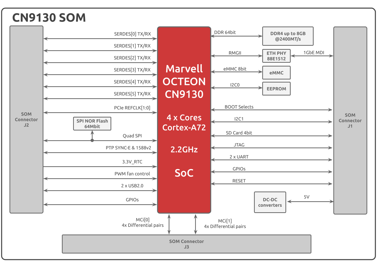
Overview
CN9130 System On Module is a highly integrated SOM module based on Marvell’s CN9130 SoC.
The SoC highlights are up to 2.2GHz with 4 Cortex A72 Arm cores, DDR4 controller and 6 high speed SERDESs.
The module integrates the following features –
CN9130 SoC (up to 2.2GHz).
On board 64bit DDR4 bus supporting up to 16GB at 2400MT/s without ECC
Single 12V or 5V DC-input is required.
Block Diagram
Specifications
Features | CN9130 SOM Specifications | ||||||||
Processor Core | 4 cores Arm Cortex A72 | ||||||||
Processor speed | 2.2GHz (Commercial) | ||||||||
DDR | On board DDR4: | ||||||||
eMMC | Up to 64GB (assembled 8GB) | ||||||||
Flash | 64Mbit SPI NOR flash | ||||||||
SATA 3.0 | up to 2 Ports | ||||||||
Ethernet | 1x MDI using 88E1512 PHY 1x 10/5 GbE port + 2x 1/2.5 GbE Ports | ||||||||
PCIe gen 3.0 | 1 Port x4 + 2 Ports x 1 | ||||||||
USB 3.0 | Up to 2 x USB 3.0 (Host/Device) | ||||||||
I2C | 2 | ||||||||
SMI & XSMI | 2 | ||||||||
UART | 2 | ||||||||
PPS/PTP support | ✓ | ||||||||
SPI bus | ✓ | ||||||||
RTC support | ✓ | ||||||||
Power | 5V to 12V DC-input | ||||||||
Supported OS | Linux kernel 5.8x Yocto DPDK UEFI KVM/QEMU/Containers NFV Openstack compute node | ||||||||
Environment | Commercial: 0°C to 70°C | ||||||||
Dimensions | 49mm X 35mm | ||||||||
|
Compatibility between SOMs A388 and CN9130
Both SOMs have exactly the same form factor and footprint
The CN9130 SOM was designed to support SolidRun’s ClearFog Base/Pro. In case of any custom design based on A388 that wants to upgrade to CN9130, any case needs to be examined individually and review carefully the borad-to-board pinout
In the documentation section there is an excel table with exact pinout difference
Main differences due to SoC pinout:
Feature | A388 | CN9130 |
USB2.0 | 3 Ports | 2 Ports |
SATA 3.0 | 3 Ports | 2 Ports |
125MHz clock out | ✓ | X |
SD/EMMC Boot | boot from SD or eMMC | Can boot from both SD or eMMC |
MCi interface | X | ✓ – Connector J3 |
input voltage | 5V and 3.3V | 5V |
Power Consumption
The following power consumption measurements were conducted on the following setup:
Clearfog Pro carrier board
Voltage / current measurement on v_5v0 voltage rail
No mPCIe / USB / SATA / ETH cable were connected to the carrier board
Temperature measurement was taken from linux using the following command
‘cat /sys/class/thermal/thermal_zone?/temp’Current and Voltage measured using an oscilloscope
Linux command ‘memtester 100M > /dev/null &’ ran 4 times according to core count
Linux command ‘cpuburn-krait’ is ran 4 times in background. The reason cpuburn-krait was chosen is since it can generate most heat out of the cores (the core pipeline are most utilized)
Freqeuncy Scaling
In order to improve power efficiency and increase temperature limits, SolidRun had enabled cpu frequency scaling.
Please refer to the patch below for more information.
https://github.com/SolidRun/cn913x_build/commit/5fe77346371a230fd2468bfb11cbcc2c1ea10345
SolidRun, recommends to not disable the frequency scaling feature.
Power Measurments
The measurements below were conducted without frequency scaling, to reflect the maximum power consumption:
Test | Power [W] | Tj [degC] |
Idle u-boot | 4.6 | 50 |
idle Linux | 4.08 | 53 |
memtester 64bit 2400MT/s | 9.25 | 70 |
cpuburn-karit 4 cores at 2.2GHz | 9.3 | 70 |
CN9130 SOM extensions
The CN9130 has two extension busses of high performance, low latency and low power Marvell® MoChi interfaces (MCi). Each bus is comprised of 4x high speed differential pairs and a dedicated LVDS clock. Both busses are exposed through the SOM connector, enabling to connect 1 or 2 additional 88F8215 comprising the kits of CN9131 and CN9132 on the carrier board and extending the SERDES count from 6 to 12 or 18.
SERDES Muxing CN9130 – CP0:
Interface | SERDES Lane0 | SERDES Lane1 | SERDES Lane2 | SERDES Lane3 | SERDES Lane4 | SERDES Lane5 |
10GBASE-R/XFI |
|
| ETH_Port0 |
| ETH_Port0 |
|
5GBASE-R |
|
| ETH_Port0 |
| ETH_Port0 or ETH_Port1 |
|
10GBASE-X2 (RXAUI) |
|
| ETH_Port0 Lane 0 | ETH_Port0 Lane 1 | ETH_Port0 Lane0 | ETH_Port0 Lane 1 |
1000BASE-X (SGMII) / 2.5GBASE-X (HS-SGMII) | ETH_Port1 | ETH_Port2 | ETH_Port0 | ETH_Port1 | ETH_Port0 or ETH_Port1 | ETH_Port2 |
SATA 3.0 | SATA1 | SATA0 | SATA0 | SATA1 |
| SATA1 |
USB 3.0 HOST |
| USB 3.0 Port0 Host | USB 3.0 Port0 Host | USB 3.0 Port1 Host | USB 3.0 Port1 Host |
|
USB 3.0 Device |
| USB 3.0 Port0 Decive |
|
| USB 3.0 Port0 Decive |
|
PCIe RC/EP | PCIex4 Port0 LANE0 | PCIex4 Port0 LANE1 | PCIex4 Port0 LANE2 | PCIex4 Port0 LANE3 | PCIex1 Port1 | PCIex1 Port2 |
CN9130 SOM default config based on Clearfog Base/Pro | PCIe X1 Port0 | USB Port0 | XFI | SGMII | PCIe Gen3 Port1 | SATA1 |
The following port configuration can’t be used simultaneously:
SGMII port 0 / HS SGMII port0, RXAUI and XFI/10GBASE
SGMII port 1 and HS SGMII port 1
SGMII port 2 and HS SGMII port 2
CORE Clock BOOT Straps
PLL_SEL[0] – MPP15 – SPI1_MOSI
PLL_SEL[1] – MPP16 – SPI1_CLK
PLL_SEL[2] – MPP17
PLL_SEL[3] – MPP45 (not exposed on B2B connector)
Core Clock [MHz] | Configuration PLL_SEL [3:0] |
1600 | 0x0000 (0h0) |
2000 | 0x0010 (0h2) |
2200 | 0x0100 (0h4) |
BOOT MODE BOOT Straps
BOOT_MODE[0] – MPP18
BOOT_MODE[1] – MPP19
BOOT_MODE[2] – MPP20, (Constant ‘0’ – not exposed on B2B connector)
BOOT_MODE[3] – MPP21
BOOT_MODE[4] – MPP22, (not exposed on B2B connector)
BOOT_MODE[5] – MPP23, (Constant ‘1’ – not exposed on B2B connector)
BOOT MODE | Configuration BOOT_MODE [5:0] |
SD Card | 0x101001 (0h29) |
eMMC | 0x101010 (0h2A) |
NOR Flash SPI 24 address bit | 0x110010 (0h32) |
CP0 MPP[62:0]
MPP # | Pin # | Pin Description | Notes |
|---|---|---|---|
AP_MPP[0] | AP10 | EMMC_CLK | 1.8V, serial 22ohm resistor |
AP_MPP[1] | AT10 | EMMC_CMD | 1.8V, 10K PU |
AP_MPP[2] | AP16 | EMMC_D0 | 1.8V, 10K PU |
AP_MPP[3] | AP18 | EMMC_D1 | 1.8V, 10K PU |
AP_MPP[4] | AT16 | EMMC_D2 | 1.8V, 10K PU |
AP_MPP[5] | AP14 | EMMC_D3 | 1.8V, 10K PU |
AP_MPP[6] | AP12 | EMMC_DS | RCLK, 10K PD |
AP_MPP[7] | AT14 | EMMC_D4 | 1.8V, 10K PU |
AP_MPP[8] | AT12 | EMMC_D5 | 1.8V, 10K PU |
AP_MPP[9] | AT18 | EMMC_D6 | 1.8V, 10K PU |
AP_MPP[10] | AV18 | EMMC_D7 | 1.8V, 10K PU |
AP_MPP[11] | AY18 | UART_AP_TX | PD - Reset strap |
AP_MPP[12] | BA17 | EMMC_RST | 1.8V, 10K PD |
AP_MPP[19] | AW17 | UART_AP_RX | 3.3V thorough NTB0102GD level shifter |
MPP[0] | AY38 | RGMII_RXD3 | |
MPP[1] | AV38 | RGMII_RXD2 | |
MPP[2] | AW39 | RGMII_RXD1 | |
MPP[3] | AY40 | RGMII_RXD0 | |
MPP[4] | AW41 | RGMII_RXCTL | |
MPP[5] | BA39 | RGMII_RXCLK | |
MPP[6] | AW35 | RGMII_TXD3 | |
MPP[7] | AY36 | RGMII_TXD2 | |
MPP[8] | BA37 | RGMII_TXD1 | |
MPP[9] | AW37 | RGMII_TXD0 | |
MPP[10] | BA35 | RGMII_TXCTL | |
MPP[11] | AV36 | RGMII_TXCLK | |
MPP[12] | AV32 | SPI1_CP0_CS1_N | |
MPP[13] | AY34 | SPI1_CP0_MISO | |
MPP[14] | AT36 | SPI1_CP0_CS0_N | |
MPP[15] | AT32 | SPI1_CP0_MOSI | CPU Subsystem Clock |
MPP[16] | AV34 | SPI1_CP0_CLK | CPU Subsystem Clock |
MPP[17] | BA29 | CP0_SYS_PLL_SEL2 | CPU Subsystem Clock |
MPP[18] | AW29 | CP0_BOOT_MODE_SEL0 | CPU Subsystem Clock |
MPP[19] | AV30 | CP0_BOOT_MODE_SEL1 | Boot mode strap |
MPP[20] | BA31 | CP0_BOOT_MODE_SEL2 | Boot mode strap |
MPP[21] | AT30 | CP0_BOOT_MODE_SEL3 | Boot mode strap |
MPP[22] | AY30 | CP0_BOOT_MODE_SEL4 | Boot mode strap |
MPP[23] | AP32 | CP0_BOOT_MODE_SEL5 / SMB_ALERT_N | Boot mode strap |
MPP[24] | AP34 | CP0_MPP24 | 3.3V |
MPP[25] | AT34 | CP0_MPP25 | Reset strap |
MPP[26] | AT38 | CP0_MPP26 | Reset strap |
MPP[27] | AW31 | CP0_MPP27 | 3.3V |
MPP[28] | AY32 | CP0_PTP_PULSE | |
MPP[29] | BA33 | CP0_PTP_CLK_IN | |
MPP[30] | AW33 | CP0_PTP_PCLK_OUT | |
MPP[31] | AP36 | CP0_MPP31 | 3.3V |
MPP[32] | H30 | CP0_MPP32 | 3.3V |
MPP[33] | C39 | CP0_MPP33 | 3.3V |
MPP[34] | C41 | CP0_MPP34 | 3.3V |
MPP[35] | F32 | I2C1_CP0_SDA | 3.3V, 2.2K PU |
MPP[36] | H32 | I2C1_CP0_SCL | 3.3V, 2.2K PU |
MPP[37] | F34 | I2C0_CP0_SCL | 3.3V, 2.2K PU |
MPP[38] | H34 | I2C0_CP0_SDA | 3.3V, 2.2K PU |
MPP[39] | F30 | CP0_MPP39 | 3.3V |
MPP[40] | F36 | RCVR1_CLK_CP0 | 3.3V, 25MHz for SYNC-E connected to J1 |
MPP[41] | H36 | VHV_EN | 3.3V, 2.2K PD |
MPP[42] | E39 | CP0_MPP42 | 3.3V |
MPP[43] | D30 | CP0_MPP43 | 3.3V |
MPP[44] | D38 | CP0_MPP44 | 1.8V, Reset Strap |
MPP[45] | A39 | CP0_MPP45 | 1.8V, Reset strap |
MPP[46] | C37 | SYS_PLL_SEL3 | CPU Subsystem Clock |
MPP[47] | A37 | SMI_CP0_MDC | 1.8V, Reset strap, PD |
MPP[48] | B40 | CP0_MPP48 | 1.8V, Reset strap |
MPP[49] | B38 | SMI_CP0_MDIO | 1.8V, 2.2K PU |
MPP[50] | C35 | UART2_TX | 3.3V thorough NTB0102GD level shifter |
MPP[51] | D34 | UART2_RX | 3.3V thorough NTB0102GD level shifter |
MPP[52] | A35 | CP0_MPP52 | 1.8V |
MPP[53] | B36 | DDR_SPD_STRAP | 1.8V, SPD DDR configuration loading from EEPROM |
MPP[54] | D36 | CP0_RCVR2_CLK | 25MHz for SYNC-E connected to PHY |
MPP[55] | B34 | SD_CARD_DETECT_N | 3.3V, 2.2K PU |
MPP[56] | D32 | SD_CLK | 3.3V |
MPP[57] | B32 | SD_CMD | 3.3V |
MPP[58] | A33 | SD_D0 | 3.3V |
MPP[59] | C33 | SD_D1 | 3.3V |
MPP[60] | A31 | SD_D2 | 3.3V |
MPP[60] | C31 | SD_D3 | 3.3V |
MPP[62] | B30 | NC |
SOM Header Details
Following are the SOM Connectors J1, J2, J3 pin mapping –
GND pins are marked with Red
The SOM has 3 connectors:
J1, J2 – DF40C-80DP-0.4V(51), 80
Mating connectors:DF40C-80DS-0.4V(51) – 1.5mm mating height
DF40C(2.0)-80DS-0.4V(51) – 2mm mating height
DF40C(4.0)-80DS-0.4V(51) – 4mm mating height
J3 – DF40C-70DP-0.4V(51), 70
Mating connectors:DF40C-70DS-0.4V(51) – 1.5mm mating height
DF40C(2.0)-70DS-0.4V(51) – 2mm mating height
DF40C(4.0)-70DS-0.4V(51) – 4mm mating height
Spacers
Manufacture PN: N0143416A (for 1.5mm stacking height)
Screw M1.6
Connector J1
Notes | Driving IC | Schematics Pin Name | Pin Number | Pin Number | Schematics Pin Name | Driving IC | Notes |
|---|---|---|---|---|---|---|---|
2 | 1 | GND (FIXED) | |||||
4 | 3 | MDI_P0 | CP0 RGMII through 88E1512 PHY | ||||
RCVR1_CLK_CP0 | 6 | 5 | MDI_N0 | CP0 RGMII through 88E1512 PHY | |||
8 | 7 | GND (FIXED) | |||||
10 | 9 | MDI_P1 | CP0 RGMII through 88E1512 PHY | ||||
12 | 11 | MDI_N1 | CP0 RGMII through 88E1512 PHY | ||||
3.3V, 2.2K PU | I2C1_CP0_SCL | 14 | 13 | GND (FIXED) | |||
3.3V | SPI1_CP0_CS1_N | 16 | 15 | MDI_P2 | CP0 RGMII through 88E1512 PHY | ||
CP0_MPP31 | 18 | 17 | MDI_N2 | CP0 RGMII through 88E1512 PHY | |||
3.3V thorough NTB0102GD level shifter, 2.2K PU | UART2_CP0_RX | 20 | 19 | GND (FIXED) | |||
3.3V | CP0_MPP32 | 22 | 21 | MDI_P3 | CP0 RGMII through 88E1512 PHY | ||
3.3V thorough NTB0102GD level shifter, 2.2K PU | UART2_CP0_TX | 24 | 23 | MDI_N3 | CP0 RGMII through 88E1512 PHY | ||
GND (FIXED) | 26 | 25 | GND (FIXED) | ||||
28 | 27 | PHY0_RST_N_1.8V | 1.8V, input reset to PHY | ||||
3.3V, Reset Strap | CP0_BOOT_MODE_SEL0 | 30 | 29 | GBE0_LED2_INT_N | 88E1512 | 1.8V, serial 510ohm resistor | |
3.3V, Reset Strap | CP0_BOOT_MODE_SEL1 | 32 | 31 | GBE0_LED1 | 88E1512 | 1.8V, serial 510ohm resistor | |
3.3V, Reset Strap | CP0_BOOT_MODE_SEL3 | 34 | 33 | GBE0_LED0 | 88E1512 | 1.8V, serial 510ohm resistor | |
SD CARD, 3.3V, 2.2K PU | SD_CP0_CD_N | 36 | 35 | SMI_CP0_MDIO | connected to PHY 88E1512 ADD 0x0 | 1.8V, 2.2K PU | |
3.3V thorough NTB0102GD level shifter, 2.2K PU | UART_AP_RX0 | 38 | 37 | SMI_CP0_MDC | connected to PHY 88E1512 ADD 0x0 | 1.8V, 2.2K PD (Reset Strap) | |
3.3V thorough NTB0102GD level shifter, 2.2K PU | UART_AP_TX0 | 40 | 39 | CP0_MPP44 | 1.8V | ||
Reset IN | SYS_RESET_N | 42 | 41 | GND (FIXED) | |||
44 | 43 | JTAG_CP0_TCK | JTAG, 3.3V, 10K PD | ||||
Reset OUT | CP0_SYSRST_OUT_N | 46 | 45 | JTAG_CP0_TRST_N | JTAG, 3.3V, 10K PD | ||
48 | 47 | JTAG_CP0_TDI | JTAG, 3.3V, 10K PU | ||||
JTAG, 3.3V, 10K PU | JTAG_CP0_TMS | 50 | 49 | JTAG_CP0_TDO | JTAG, 3.3V, 10K PU | ||
52 | 51 | CP0_MPP24 | 3.3V | ||||
SD CARD, 3.3V | SD_CP0_SDIO_D0 | 54 | 53 | SD_CP0_SDIO_CMD | SD CARD, 3.3V | ||
SD CARD, 3.3V | SD_CP0_SDIO_D3 | 56 | 55 | SD_CP0_SDIO_CLK | SD CARD, 3.3V | ||
58 | 57 | CP0_MPP27 | 3.3V | ||||
SD CARD, 3.3V | SD_CP0_SDIO_D1 | 60 | 59 | GND (FIXED) | |||
SD CARD, 3.3V | SD_CP0_SDIO_D2 | 62 | 61 | I2C1_CP0_SDA | 3.3V, 2.2K PU | ||
64 | 63 | ||||||
3.3V, 2.2K PU | EEPROM 0x53 | I2C0_CP0_SDA | 66 | 65 | |||
3.3V, 2.2K PU | EEPROM 0x53 | I2C0_CP0_SCL | 68 | 67 | |||
3.3V | PTP_CP0_PULSE | 70 | 69 | VIN | 12V or 5V | ||
3.3V | PTP_CP0_CLK_IN | 72 | 71 | VIN | 12V or 5V | ||
3.3V | PTP_CP0_PCLK_OUT | 74 | 73 | VIN | 12V or 5V | ||
1.8V | CP0_MPP52 | 76 | 75 | VIN | 12V or 5V | ||
78 | 77 | VIN | 12V or 5V | ||||
80 | 79 | VIN | 12V or 5V |
Connector J2
Notes | Driving IC | Schematics Pin Name | Pin Number | Pin Number | Schematics Pin Name | Driving IC | Notes |
|---|---|---|---|---|---|---|---|
No on-board serial capacitor | B2B_SRD2_TX_P | 2 | 1 | GND (FIXED) | |||
No on-board serial capacitor | B2B_SRD2_TX_N | 4 | 3 | USB2_CP0_DP1 | |||
GND (FIXED) | 6 | 5 | USB2_CP0_DM1 | ||||
No on-board serial capacitor | B2B_SRD2_RX_P | 8 | 7 | GND (FIXED) | |||
No on-board serial capacitor | B2B_SRD2_RX_N | 10 | 9 | ||||
GND (FIXED) | 12 | 11 | |||||
No on-board serial capacitor | B2B_SRD4_RX_P | 14 | 13 | GND (FIXED) | |||
No on-board serial capacitor | B2B_SRD4_RX_N | 16 | 15 | USB2_CP0_DP0 | |||
GND (FIXED) | 18 | 17 | USB2_CP0_DM0 | ||||
No on-board serial capacitor | B2B_SRD4_TX_P | 20 | 19 | CP0_MPP33 | 3.3V | ||
No on-board serial capacitor | B2B_SRD4_TX_N | 22 | 21 | ||||
GND (FIXED) | 24 | 23 | 3.3V_RTC_B2B | 3.3V battery voltage | |||
No on-board serial capacitor | B2B_SRD1_TX_P | 26 | 25 | PCIE_REFCLK_N1 | 100MHz HCSL clock out, no serial capacitors | ||
No on-board serial capacitor | B2B_SRD1_TX_N | 28 | 27 | PCIE_REFCLK_P1 | 100MHz HCSL clock out, no serial capacitors | ||
GND (FIXED) | 30 | 29 | GND (FIXED) | ||||
No on-board serial capacitor | B2B_SRD1_RX_P | 32 | 31 | PCIE_REFCLK_P0 | 100MHz HCSL clock out, no serial capacitors | ||
No on-board serial capacitor | B2B_SRD1_RX_N | 34 | 33 | PCIE_REFCLK_N0 | 100MHz HCSL clock out, no serial capacitors | ||
GND (FIXED) | 36 | 35 | GND (FIXED) | ||||
No on-board serial capacitor | B2B_SRD5_RX_P | 38 | 37 | ||||
No on-board serial capacitor | B2B_SRD5_RX_N | 40 | 39 | ||||
GND (FIXED) | 42 | 41 | |||||
No on-board serial capacitor | B2B_SRD5_TX_P | 44 | 43 | CP0_SYS_PLL_SEL2 | Boot strap | ||
No on-board serial capacitor | B2B_SRD5_TX_N | 46 | 45 | CP0_MPP34 | 3.3V | ||
GND (FIXED) | 48 | 47 | CP0_MPP43 | 3.3V | |||
No on-board serial capacitor | B2B_SRD3_TX_P | 50 | 49 | ||||
No on-board serial capacitor | B2B_SRD3_TX_N | 52 | 51 | ||||
GND (FIXED) | 54 | 53 | |||||
No on-board serial capacitor | B2B_SRD3_RX_P | 56 | 55 | ||||
No on-board serial capacitor | B2B_SRD3_RX_N | 58 | 57 | CP0_MPP42 | 3.3V | ||
GND (FIXED) | 60 | 59 | |||||
No on-board serial capacitor | B2B_SRD0_RX_P | 62 | 61 | ||||
No on-board serial capacitor | B2B_SRD0_RX_N | 64 | 63 | 1.8V_VHV | NC | ||
GND (FIXED) | 66 | 65 | 1.8V_OUT | Option to provide 1.8V out for low power misc logic | |||
No on-board serial capacitor | B2B_SRD0_TX_P | 68 | 67 | 1.8V_OUT | Option to provide 1.8V out for low power misc logic | ||
No on-board serial capacitor | B2B_SRD0_TX_N | 70 | 69 | ||||
GND (FIXED) | 72 | 71 | |||||
74 | 73 | CP0_MPP39 | 3.3V | ||||
76 | 75 | ||||||
3.3V | SPI1_CP0_MISO | 78 | 77 | SPI1_CP0_MOSI | 3.3V, Boot Strap | ||
3.3V | SPI1_CP0_CS0_N | 80 | 79 | SPI1_CP0_CLK | 3.3V, Boot Strap |
Connector J3
Notes | Driving IC | Schematics Pin Name | Pin Number | Pin Number | Schematics Pin Name | Driving IC | Notes |
|---|---|---|---|---|---|---|---|
GND (FIXED) | 2 | 1 | GND (FIXED) | ||||
No on-board serial capacitor | AP_MCI0_RX_CP1_N2 | 4 | 3 | AP_MCI0_TX_CP1_P0 | No on-board serial capacitor | ||
No on-board serial capacitor | AP_MCI0_RX_CP1_P2 | 6 | 5 | AP_MCI0_TX_CP1_N0 | No on-board serial capacitor | ||
GND (FIXED) | 8 | 7 | GND (FIXED) | ||||
No on-board serial capacitor | AP_MCI0_RX_CP1_N1 | 10 | 9 | REFCLK_MCI0_CP1_N | No on-board serial capacitor | ||
No on-board serial capacitor | AP_MCI0_RX_CP1_P1 | 12 | 11 | REFCLK_MCI0_CP1_P | No on-board serial capacitor | ||
GND (FIXED) | 14 | 13 | GND (FIXED) | ||||
No on-board serial capacitor | AP_MCI0_RX_CP1_N0 | 16 | 15 | AP_MCI0_TX_CP1_P1 | No on-board serial capacitor | ||
No on-board serial capacitor | AP_MCI0_RX_CP1_P0 | 18 | 17 | AP_MCI0_TX_CP1_N1 | No on-board serial capacitor | ||
GND (FIXED) | 20 | 19 | GND (FIXED) | ||||
No on-board serial capacitor | AP_MCI0_RX_CP1_P3 | 22 | 21 | AP_MCI0_TX_CP1_P2 | No on-board serial capacitor | ||
No on-board serial capacitor | AP_MCI0_RX_CP1_N3 | 24 | 23 | AP_MCI0_TX_CP1_N2 | No on-board serial capacitor | ||
GND (FIXED) | 26 | 25 | GND (FIXED) | ||||
No on-board serial capacitor | 28 | 27 | AP_MCI0_TX_CP1_P3 | No on-board serial capacitor | |||
30 | 29 | AP_MCI0_TX_CP1_N3 | No on-board serial capacitor | ||||
No on-board serial capacitor | GND (FIXED) | 32 | 31 | GND (FIXED) | |||
34 | 33 | ||||||
36 | 35 | 5V_MGT | Connected to on board STM32 for management | ||||
38 | 37 | POWER_OFF | 3.3V, connected to EFUSE | ||||
GND (FIXED) | 40 | 39 | GND (FIXED) | ||||
Connected to on board STM32 for management | USB_MCU_DP | 42 | 41 | AP_MCI1_TX_CP2_P3 | No on-board serial capacitor | ||
Connected to on board STM32 for management | USB_MCU_DM | 44 | 43 | AP_MCI1_TX_CP2_N3 | No on-board serial capacitor | ||
GND (FIXED) | 46 | 45 | GND (FIXED) | ||||
No on-board serial capacitor | AP_MCI1_RX_CP2_P0 | 48 | 47 | AP_MCI1_TX_CP2_N0 | No on-board serial capacitor | ||
No on-board serial capacitor | AP_MCI1_RX_CP2_N0 | 50 | 49 | AP_MCI1_TX_CP2_P0 | No on-board serial capacitor | ||
GND (FIXED) | 52 | 51 | GND (FIXED) | ||||
No on-board serial capacitor | AP_MCI1_RX_CP2_P1 | 54 | 53 | REFCLK_MCI1_CP2_N | No on-board serial capacitor | ||
No on-board serial capacitor | AP_MCI1_RX_CP2_N1 | 56 | 55 | REFCLK_MCI1_CP2_P | No on-board serial capacitor | ||
GND (FIXED) | 58 | 57 | GND (FIXED) | ||||
No on-board serial capacitor | AP_MCI1_RX_CP2_P3 | 60 | 59 | AP_MCI1_TX_CP2_P1 | No on-board serial capacitor | ||
No on-board serial capacitor | AP_MCI1_RX_CP2_N3 | 62 | 61 | AP_MCI1_TX_CP2_N1 | No on-board serial capacitor | ||
GND (FIXED) | 64 | 63 | GND (FIXED) | ||||
No on-board serial capacitor | AP_MCI1_RX_CP2_N2 | 66 | 65 | AP_MCI1_TX_CP2_N2 | No on-board serial capacitor | ||
No on-board serial capacitor | AP_MCI1_RX_CP2_P2 | 68 | 67 | AP_MCI1_TX_CP2_P2 | No on-board serial capacitor | ||
GND (FIXED) | 70 | 69 | GND (FIXED) |
Heatsink
SolidRun provides few types of heatsinks:
Cool-plate: flattens the surface of the SOM, making it easier for integration in any enclosure design
Evaluation heatsink: add-on for the cool-plate, with short ribs, enabling to mount a 40mmX40mm fan. This heatsink is to be used in open frame systems, to enable developers to work with the CN9130 SOM during bring-up and software development
Documentation
| Attachments | ||||
|---|---|---|---|---|
|
| Ui button | ||||||
|---|---|---|---|---|---|---|
|