Revisions and Notes
Date | Owner | Revision | Notes | ||||||||
| Noam Weidenfeld | 1.0 | |||||||||
Table of Contents |
| ||||||||||
| Info |
|---|
...
Disclaimer No warranty of accuracy is given concerning the contents of the information contained in this publication. To the extent permitted by law no liability (including liability to any person by reason of negligence) will be accepted by SolidRun Ltd., its subsidiaries or employees for any direct or indirect loss or damage caused by omissions from or inaccuracies in this document. SolidRun Ltd. reserves the right to change details in this publication without prior notice. Product and company names herein may be the trademarks of their respective owners. |
Introduction
This User Manual relates to the SolidRun SR-SOM-AM64xx-series, which includes
Single/Dual core ARM A53 (1.0 GHz).
Single/Dual cores Cortex®-R5F 800 MHz processor.
A general-purpose Cortex®-M4F 400 MHz processor.
Overview
The SolidRun’s SR-SOM-AM64xx is a low power, low-cost high performance micro system on module (S.O.M.) based on the highly integrated TI's AM64xx family of products targeting the Industrial Market Applications.
Highlighted Features
Ultra-small footprint SOM (47x30mm) including three board-to-board connectors (250 total pins number).
TI's AM64XX SoC:
- Single/Dual core Cortex A53 up to 1.0GHz
- 400 MHz Cortex-M4F subsystem processor supports real time tasks.
- Up to two dual-core Cortex-R5F MCU subsystems at up to 800 MHz, integrated for real-time processing.
- Safety & Security enginesDDR4 (1.6 GHz) memory in x16 configurations supports up to 2GB and inline ECC
Up to two 1GB Ethernet port supporting Industrial Ethernet protocols.
Single Gigabit Ethernet interface.
Two ports TSN GE switch.
Industrial IO supports – CAN, RS-485 etc.
Single PCIe Gen 2 or USB 3 interface.
Low latency interfaces to motor control front.
Supporting Products
The following products are provided from SolidRun both as production level platforms and as reference examples on how to incorporate the SOM in different levels of integration:
HummingBoard AM64x– A board computer that incorporates the SOM retains the same Linux distributions while adding extra hardware functionalities and access to the hardware.
Description
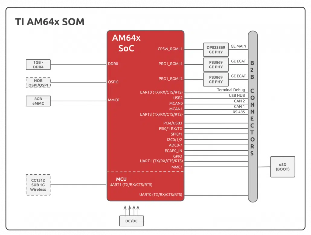
Block Diagram
The following figure describes the AM64xx SOM's Blocks Diagram.
Features Summary
Following is the features summary of the SOM. Notice that some of the features are pinout multiplexed (please refer to the pin mux table and the TI's AM64xx data sheets):
· Dual/Single ARM® Cortex™ A53 Processor, up to 1.0 GHz
· Dual or single dual-core Cortex R5F Up to 800 MHz
· Cortex-M4 subsystem processor up to 400 MHz
· Up to 2GByte DDR4 memory
· Up to 64 GB eight bits eMMC memory.
· OSPI/QSPI NOR Flash memory.
· I2C EEPROM.
· Up to 3 x 10/100/1000 Mbps Ethernet PHY
o Up to two gigabit Industrial Communication Subsystems e.g., ECAT, Profinet etc.
o Time stamping
o TSN
· SUB Giga modem (CC1312)
· Variety of interfaces and IO on Board-to-Board connectors.
A single 5.0V interface
Core System Components
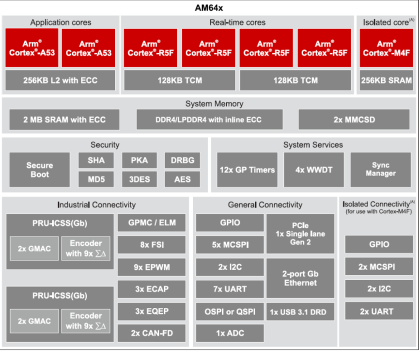
AM64xx Sitara SoC Family
The AM64xx Sitara processors feature advanced implementation of a duad Arm® Cortex®-A53 core, which operates at speeds of up to 1.0 GHz. A general-purpose Cortex®-M4 core processor is for low-power processing and two dual-core Cortex-R5F supporting industrial protocols.
The following figure describes the AM64xx main features (For more details refer to TI’s AM64x datasheet).
Memories
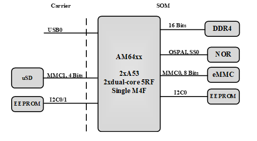
The AM64xx SOM supports varieties of memory interfaces for booting and data storage. The following figure describes the AM64xx SOM memory interfaces.
DDR4
Up to 2GB memory space.
16 Bits data bus.
Up to 1600 MT/s.
Inline ECC.
eMMC NAND Flash
Up to 64GB memory space.
8 Bits data bus.
Support of eMMC5.1 Host Specification (JESD84-B51).
HS200 SDR: 1.8 V, 0-200 MHz, 8/4-bit bus width, 200/100 MB/s
HS400 DDR is NOT supported.
Can be used as BOOT NVM *
Octal Serial NOR Flash (SOM)
Supports 1/2/4 or 8-bit operation.
Support for DDR Mode and DTR protocol.
Programmable device sizes
DMA NOT supported.
In Octal-SPI and Quad-SPI mode, Mode 1, 2, and 3 are NOT supported.
Can be used as BOOT NVM *
EEPROM (SOM)
· 1Kb EEPROM
· ON-Semi’s CAT24AA01TDI or compatible
· Address 0X50 (7 bits format)
· Stores SOM’s configurations.
Micro-SD (Carrier)
· Optional on Carrier board
· Implements 4 data bits.
· SD Host Controller Standard Specification 4.10 and SD Physical Layer Specification v3.01.
· SDIO Specification v3.00
· DDR50: UHS-I 1.8 V signalling, frequency up to 50 MHz, up to 50 MBps.
· SDR104 is NOT supported.
· Can be used as BOOT NVM *
| Note |
|---|
*Note – All boot configuration signals are available on the SOM connector. |
10/100/1000 Mbps Ethernet Interfaces
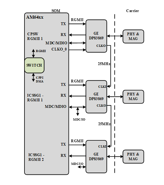
The AM64xx SOM supports three Giga-Ethernet interfaces. One of the interfaces is connected directly to the Ethernet switch (CPSW3G) and the two others are part of the Programmable Real-Time Unit and Industrial Communication Subsystem – Gigabit (PRU_ICSSG). The following figure describes the Ethernet port interfaces.
The three Giga Ethernet PHY are TI’s DP83869:
Low RGMII Latency
Low Power Consumption
Time Sensitive Network (TSN) Compliant
IEEE1588 Support
Cable Diagnostics
Recovered Clock Output for SyncE
MDI or MDIX support.
PRU_ICSSG
Two Real-Time Ethernet ports.
MDIO port to control external Ethernet PHY
Time Stamping support.
Industrial protocols used in master and slave mode, such as:
o EtherCAT®
o PROFINET™
o EtherNet/IP™
o Others
CPSW3G
Single Giga Ethernet port
Synchronous 10/100/1000 Mbit operation
MDIO port to control external Ethernet PHY
Support for Audio/Video Bridging (P802.1Qav/D6.0 and 802.1Qaz)
Support for IEEE 1588 Clock Synchronization (2008 Annex D, Annex E and Annex F)
IPV4/IPV6 UDP/TCP checksum offload.
Clock Chaining
The following figure describes the Ethernet reference clock configuration.
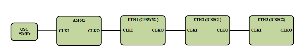
The 25Mhz clock source is the CPU’s CLOCOUT1 signal. It is connected to the CPCW3G Ethernet PHY.
ICSSG1 clock is connected to CPSW3G output clock and ICSSG2 is connected to ICSSG1 clock.
| Note |
|---|
Note – Clock need to be active before reset signal is de-asserts |
AM64xx External Interfaces
General
The SOM incorporates three Hirose DF40 board-to-board headers.
The selection of the Hirose DF40 is due to the following criteria:
· Miniature (0.4m pitch)
· Highly reliable manufacturer
· Availability (worldwide distribution channels)
· Excellent signal integrity (supports 6Gbps)
o Please contact Hirose or SolidRun for reliability and test result data.
· Mating height of between 1.5mm to 3.0mm. AM64xx headers are fixed, the final mating height is determined by carrier implementation
Supported Interfaces - Main
PCIe & USB3
The AM64xx supports a single Ser/Des interface. The Ser/Des can be configured as a PCIe or a USB3.0 interface. The following figure describes the optional Ser/Des configurations.
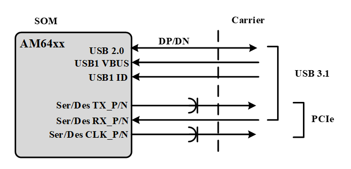
The PCIe main features are:
· Ser/Des is configured as PCIe.
· On board coupling capacitors for TX and CLK.
· PCIe clock is generated on the AM64xx SoC.
· Single PCIe lane up to 5.0GT/lane.
· Gen2 (5 Gbps 8/10-bit encoding), and Gen1 (2.5 Gbps 8/10-bit encoding) with auto-negotiation.
· Compliant to PCI-Express® Base Specification, Revision 4.0 (Version 0.7).
· PHY Interface for the PCI Express Architecture, Version 4.2 compliance.
· Supports Spread Spectrum Clocking in Transmitter and Receiver.
USB main features are:
· Ser/Des is configured as USB 3.1.
· Universal Serial Bus 3.1 (USB) subsystem with integrated USB2.0 PHY
· Dual-Role Device (DRD) capability
· Compliance with USB 3.1 Gen1 Specification
· Support of Peripheral (aka Device) mode at Super Speed (SS at 5 Gbps), High Speed (HS at 480 Mbps), and Full Speed (FS at 12 Mbps)
· Support of Host mode at Super Speed (SS at 5 Gbps), High Speed (HS at 480 Mbps), Full Speed (FS at 12 Mbps), and Low Speed (LS at 1.5 Mbps)
· ECC on internal RAMs
| Note |
|---|
NOTE – USB 2.0 is always available even if the Ser/Des is configured as PCIe. |
UART
The AM64xx SOM can support up to 4 UART interfaces. The following figure describes the UART interfaces.
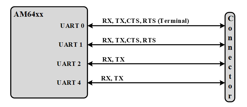
The UART interfaces main features are:
· UART 0 supports TX, RX, CTS and RTS. After POR it is used as terminal.
· UART 2 supports TX, RX, CTS and RTS.
· UART 3 Supports TX, RX, CTS and RTS.
· UART 4 support TX, RX
· RS-485 external transceiver auto flow control support.
· Baud rates up to 3.6 Mbps. Auto-baud between 1200 bits/s and 115.2 Kbits/s.
· Flow control: Hardware (RTS/CTS) or software (XON/XOFF).
· Optional multi-drop transmission.
| Note |
|---|
Note – The UART signals are multiplexed with other functional options. Refer to the Pin MUX tools for optional functionalities. |
eSPI
The AM64xx SOM supports two eSPI interface. The following figure describes the eSPI interface.
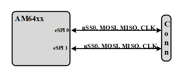
· Single HW chip select nSS0.
· Master/Slave configurable.
· Serial clock with programmable frequency, polarity, and phase for each channel.
| Note |
|---|
Note – The eSPI signals are multiplexed with other functional options. Refer to the Pin MUX tools for optional functionalities. |
I2C
The AM64xx SOM supports up to two I2C Interfaces. The following figure describes the I2C interfaces.
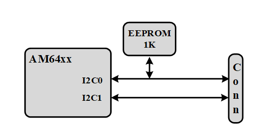
The I2C main features are:
· I2C-0 is connected to the SOM EEPROM and BtB connector.
· I2C-1 is available on the connector by default.
· Pull-up resistors assembled on SOM.
· Multi-master operation.
· In Standard mode, I2C supports the data transfer rates up to 100 kbits/s.
· In Fast mode, data transfer rates up to 400 kbits/s can be achieved.
| Note |
|---|
Note – The I2C signals are multiplexed with other functional options. Refer to the Pin MUX tools for optional functionalities. |
uSD
The uSD supports the following features:
· AM64xx’s MMC-1.
· Optional on Carrier board
· Implements 4 data bits.
· SD Host Controller Standard Specification 4.10 and SD Physical Layer Specification v3.01.
· SDIO Specification v3.00
· DDR50: UHS-I 1.8 V signalling, frequency up to 50 MHz, up to 50 MBps.
· SDR104 is NOT supported.
· Can be used as BOOT NVM *
| Note |
|---|
Note – The SDIO signals are multiplexed with other functional options. Refer to the Pin MUX tools for optional functionalities. |
MCAN
The AM64xx supports up to two CAN interfaces.
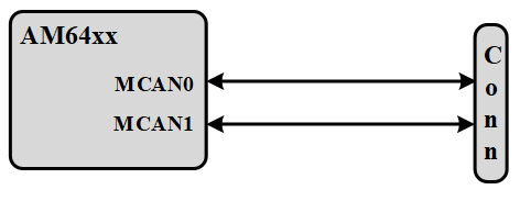
MCAN main features are:
· Conforms with CAN Protocol 2.0 A, B and ISO 11898-1:2015.
· Full CAN FD support (up to 64 data bytes).
| Note |
|---|
Note – The MCAN signals are multiplexed with other functional options. Refer to the Pin MUX tools for optional functionalities. |
ADC
The AM64xx support up to eight Analog to Digital lines. The Analog-to-Digital Converter (ADC) module contains a single 12-bit ADC which can be multiplexed to any 1of 8 analog inputs (channels).
· 4 MSPS rate with a 60 MHz SMPL_CLK.
· Functional Internal Diagnostic Debug Mode.
· Single-ended or differential input options.
· Simultaneous sampling is NOT supported.
GPIO
The AM64xx support GPIO interfaces that can be multiplex with alternative function interfaces. Some of the interfaces are:
· Fast serial interface (FSI).
· Enhanced Capture Module.
· Enhanced PWM.
· Timers
· More
| Info |
|---|
Refer to the Pin MUX tools for optional functionalities. |
Connector’s Signal Description
J5001
PIN | AM64xx SOM |
| TI Carrier |
|
| PIN | AM64xx SOM |
| TI Carrier |
|---|---|---|---|---|---|---|---|---|---|
1 | BOOTMODE0 (GPIO0_15) | 3V3 | NC |
|
| 2 | BOOTMODE13//FSI_RX1_D1 (GPIO0_28) | 3V3 | PU/PD (R88/R99) |
3 | BOOTMODE3 (GPIO0_18) | 3V3 | DIP-Switch (S1-12, PD) |
|
| 4 | BOOTMODE12//FSI_RX1_D0 (GPIO0_27) | 3V3 | PU/PD (R89/R100) |
5 | BOOTMODE1 (GPIO0_16) | 3V3 | NC |
|
| 6 | BOOTMODE11/FSI_RX1_CLK (GPIO0_26) | 3V3 | PU/PD (R90/R101) |
7 | PRG0_MDIO0_MDIO (GPIO1_40) | 3V3 | PCIe_SEL (M1 or M2 Select) |
|
| 8 | GPIO0_12 | 1V8 | M.2_RESET# (M2-67) |
9 | BOOTMODE5 (GPIO0_83) | 3V3 | DIP-Switch (S1-10, PD) |
|
| 10 | GPMC0_DIR (GPIO0_40) | 3V3 | PROCHOTn (Battery Charger, U3-11) |
11 | BOOTMODE4 (GPIO0_82) | 3V3 | DIP-Switch (S1-11, PD) |
|
| 12 | BOOTMODE9/FSI_RX0_D0 (GPIO0_24) | 3V3 | DIP-Switch (S1-7, PD) |
13 | GND |
| GND |
|
| 14 | BOOTMODE8/FSI_RX0_CLK (GPIO0_23) | 3V3 | DIP-Switch (S1-8, PD) |
15 | BOOTMODE7 (GPIO0_22) | 3V3 | PU/PD (R87/R98) |
|
| 16 | GND |
| GND |
17 | BOOTMODE6 (GPIO0_21) | 3V3 | DIP-Switch (S1-9, PD) |
|
| 18 | GPMC0_ADVn_ALE (GPIO0_32) | 3V3 | M.2_W_DIS# (M2-8) |
19 | PRG0_MDIO0_MDC (GPIO1_41) | 3V3 | PCIe_EN (Enable PCIe) |
|
| 20 | PRG0_PRU0GPO5/UART3_RTSn | 3V3 | RS-485-RE#/DE (U18-2/3) |
21 | BOOTMODE2 (GPIO0_17) | 3V3 | NC |
|
| 22 | GND |
| GND |
23 | GPCM0_WEN (GPIO0_34) | 3V3 | M.2_GPS_BT_EN# (M2-26) |
|
| 24 | PRG0_PRU1GPO6 | 3V3 | EXTENDER (J5-17) |
25 | PRG0_PRU1GPO5 | 3V3 | EXTENDER (J5-15) |
|
| 26 | PRG0_PRU0GPO15 | 3V3 | PERST# (M2-50, M1-52) |
27 | PRG0_PRU0GPO1 | 3V3 | EXTENDER (J5-33) |
|
| 28 | PRG0_PRU1GPO13 | 3V3 | EXTENDER (J5-21) |
29 | PRG0_PRU0GPO13 | 3V3 | EXTENDER (J5-7) |
|
| 30 | PRG0_PRU1GPO14 | 3V3 | EXTENDER (J5-14) |
31 | PRG1_IEP0_EDC_SYNC_OUT2 | 3V3 | NC |
|
| 32 | PRG0_PRU1GPO15 | 3V3 | CLKREQ1# (M2-52) |
33 | GND |
| GND |
|
| 34 | GPIO1_78 | 3V3 | VPP_LDO_EN (SoC Programming power enable) |
35 | PRG0_PRU1GPO3 | 3V3 | EXTENDER (J5-12) |
|
| 36 | GND |
| GND |
37 | PRG0_PRU0GPO16 | 3V3 | PCIe2_OE# (PCIe Clock2 EN) |
|
| 38 | NC |
| NC |
39 | PRG0_PRU0GPO19/UART3_RXD | 3V3 | RS-485-R (U18-1) |
|
| 40 | PRG0_PRU1GPO2 | 3V3 | EXTENDER (J5-31) |
41 | GPMC0_WAIT0 (GPIO0_37) | 3V3 | TAMPER (Sensors INT.) |
|
| 42 | PRG0_PRU0GPO6 | 3V3 | EXTENDER (J5-26) |
43 | PRG0_PRU0GPO0 | 3V3 | EXTENDER (J5-32) |
|
| 44 | PRG0_PRU1GPO1 | 3V3 | EXTENDER (J5-22) |
45 | PRG0_PRU1GPO0 | 3V3 | EXTENDER (J5-23) |
|
| 46 | PRG0_PRU0GPO3/UART3_CTSn | 3V3 | |
47 | GND |
| GND |
|
| 48 | PRG0_PRU0GPO2 | 3V3 | NC |
49 | PRG0_PRU1GPO16 | 3V3 | NC |
|
| 50 | PRG0_PRU0GPO11 | 3V3 | CLKREQ2# (M1-53) |
51 | PRG0_PRU0GPO12 | 3V3 | EXTENDER (J5-6) |
|
| 52 | GND |
| GND |
53 | PRG0_PRU0GPO8 | 3V3 | PCIe1_OE# (PCIe Clock1 EN) |
|
| 54 | PRG0_PRU0GPO4/UART3_TXD | 3V3 | RS-485-D (U18-4) |
55 | PRG0_PRU0GPO7 | 3V3 | EXTENDER (J5-16) |
|
| 56 | PRG0_PRU0GPO18 | 3V3 | NC |
57 | GND |
| GND |
|
| 58 | PRG0_PRU1GPO12 | 3V3 | EXTENDER (J5-18) |
59 | PRG0_PRU1GPO8 | 3V3 | EXTENDER (J5-20) |
|
| 60 | PRG0_PRU0GPO17 | 3V3 | PCIe_3V3_EN (M.2 PWR_EN) |
61 | PRG0_PRU1GPO4 | 3V3 | EXTENDER (J5-13) |
|
| 62 | PRG0_PRU1GPO11 | 3V3 | EXTENDER (J5-19) |
63 | GND |
| GND |
|
| 64 | GND |
| GND |
65 | PRG0_PRU0GPO14 | 3V3 | PCIe0_OE# (PCIe Clock0 EN) |
|
| 66 | SoC_WARM_RESETZ | 3V3 | NC |
67 | PRG1_IEP0_EDC_LATCH_IN0 | 3V3 | NC |
|
| 68 | NC |
| NC |
69 | PRG1_IEP0_EDC_SYNC_OUT0 | 3V3 | NC |
|
| 70 | NC |
| NC |
J7
PIN | AM64xx SOM |
| TI Carrier |
|
| PIN | AM64xx SOM |
| TI Carrier |
|---|---|---|---|---|---|---|---|---|---|
1 | GPMC0_BE1n/I2C2_SDA (GPIO0_44) | 3V3 | RTC_INT# (Real-Time-Clock INT) |
|
| 2 | GPMC0_BE1n/FSI_TX0_CLK (GPIO0_37) | 3V3 | NC |
3 | GPMC0_WAIT1/FSI_TX1_D1 (GPIO0_38) | 3V3 | EXTENDER (J5-2) |
|
| 4 | GPMC0_CSn1 (GPIO0_42) | 3V3 | USB-HUB_RST# |
5 | BOOTMODE15/FSI_TX0_D1 (GPIO0_30) | 3V3 | LED2 |
|
| 6 | GND |
| GND |
7 | BOOTMODE14/FSI_TX0_D0 (GPIO0_29) | 3V3 | LED1 |
|
| 8 | GPMC0_CSn0 (GPIO0_41) | 3V3 | CHRG_OK (Battery Charger, U3-4) |
9 | ADC0_AIN3 | 1V8 | NC |
|
| 10 | GPMC0_BE1n/I2C2_SCL (GPIO0_43) | 3V3 | WDI (Watch-Dog-IN, U17-2) |
11 | ADC0_AIN0 | 1V8 | EXTENDER (J5-38) |
|
| 12 | BOOTMODE10/FSI_RX0_D1 (GPIO0_25) | 3V3 | PU/PD (R91/R102) |
13 | ADC0_AIN1 | 1V8 | EXTENDER (J5-39) |
|
| 14 | ADC0_AIN2 | 1V8 | EXTENDER (J5-40) |
15 | ADC0_AIN7 | 1V8 | NC |
|
| 16 | GPMC0_OEn_REn (GPIO0_33) | 3V3 | LED3 |
17 | GND |
| GND |
|
| 18 | ADC0_AIN4 | 1V8 | NC |
19 | SoC_I2C0_SCL | 3V3 | Semsors, Battery Charger |
|
| 20 | GPMC0_CLK (GPIO0_31) |
| NC |
21 | SoC_I2C0_SDA | 3V3 | Semsors, Battery Charger |
|
| 22 | GPMC0_BE0n_CLE/FSI_TX1_D0 (GPIO0_35) |
| EXTENDER (J5-3) |
23 | GND |
| GND |
|
| 24 | ADC0_AIN5 | 1V8 | NC |
25 | SYNC1_OUT_TP (GPIO1_68) | 3V3 | NC |
|
| 26 | ADC0_AIN6 | 1V8 | NC |
27 | SoC_I2C1_SCL | 3V3 | RTC, EXTENDER (J5-25) |
|
| 28 | GPMC0_WPn/FSI_TX1_CLK (GPIO0_39) |
| EXTENDER (J5-1) |
29 | SoC_I2C1_SDA | 3V3 | RTC, EXTENDER (J5-24) |
|
| 30 | RESETSTATz | 3V3 | RESETSTATz |
31 | HSE_MCAN1_RX/I2C3_SDA (GPIO1_63) | 3V3 | HSE_MCAN1_RX (U19-4) |
|
| 32 | MCU_SAFETY_ERRORz_1V8 | 1V8 | NC |
33 | HSE_MCAN1_TX/I2C3_SCL (GPIO1_62) | 3V3 | HSE_MCAN1_TX (U19-1) |
|
| 34 | PORz_OUT | 3V3 | PORz_OUT |
35 | GND |
| GND |
|
| 36 | SoC_CLKIN | 1V8 | NC |
37 | HSE_MCAN0_RX/UART4_TXDL (GPIO1_61) | 3V3 | HSE_MCAN0_RX (U20-4) |
|
| 38 | SOC_MAIN_UART0_CTS_3V3 (GPIO1_54) | 3V3 | NC |
39 | HSE_MCAN0_TX/UART4_RXD (GPIO1_60) | 3V3 | HSE_MCAN0_TX (U20-1) |
|
| 40 | SOC_MAIN_UART0_RTS_3V3 (GPIO1_55) | 3V3 | NC |
41 | GND |
| GND |
|
| 42 | GND |
| GND |
43 | SOC_MAIN_UART3_RX_3V3/UART1_CTS (GPIO1_58) | 3V3 | EXTENDER (J5-29) |
|
| 44 | MCU_RESETSTATz | 3V3 | NC |
45 | SOC_MAIN_UART3_TX_3V3/UART1_RTS (GPIO1_59) | 3V3 | EXTENDER (J5-27) |
|
| 46 | SOC_SPI1_CLK (GPIO1_49) | 3V3 | NC |
47 | SOC_MAIN_UART1_RX_3V3 (GPIO1_56) | 3V3 | EXTENDER (J5-30) |
|
| 48 | SOC_SPI1_MOSI (GPIO1_50) | 3V3 | NC |
49 | SOC_MAIN_UART1_TX_3V3 (GPIO1_57) | 3V3 | EXTENDER (J5-28) |
|
| 50 | SOC_SPI1_MISO (GPIO1_51) | 3V3 | NC |
51 | SOC_SPI0_CLK (GPIO1_44) | 3V3 | EXTENDER (J5-8) |
|
| 52 | SOC_MAIN_UART0_TX_3V3 (TERMINAL) | 3V3 | TERMINAL |
53 | SOC_SPI0_MISO (GPIO1_46) | 3V3 | EXTENDER (J5-9) |
|
| 54 | SOC_MAIN_UART0_RX_3V3 (TERMINAL) | 3V3 | TERMINAL |
55 | SOC_SPI0_MOSI (GPIO1_45) | 3V3 | EXTENDER (J5-10) |
|
| 56 | SOC_SPI1_CS0 (GPIO1_51) | 3V3 | NC |
57 | SOC_SPI0_CS0 (GPIO1_42) | 3V3 | EXTENDER (J5-11) |
|
| 58 | SOC_SPI1_CS1 (GPIO1_48) | 3V3 | NC |
59 | SOC_SPI0_CS1 (GPIO1_43) | 3V3 | NC |
|
| 60 | MCU_I2C1_SDA (MCU_GPIO0_21) | 3V3 | NC |
61 | GND |
| GND |
|
| 62 | MCU_I2C0_SCL | 3V3 | NC |
63 | MCU_I2C1_SCL (MCU_GPIO0_20) | 3V3 | NC |
|
| 64 | MCU_I2C0_SDA | 3V3 | NC |
65 | PORz | OD | PORz (Push Button) |
|
| 66 | MCU_UART0_RX_3V3 (MCU_GPIO0_3) | 3V3 | NC |
67 | MCU_UART0_RTS_3V3 (MCU_GPIO0_0) | 3V3 | NC |
|
| 68 | MCU_UART0_TX_3V3 (MCU_GPIO0_23) | 3V3 | NC |
69 | MCU_UART0_CTS_3V3 (MCU_GPIO0_1) | 3V3 | NC |
|
| 70 | GND |
| GND |
71 | MCU_SPI1_MISO (MCU_GPIO0_9) | 3V3 | NC |
|
| 72 | MCU_SPI1_CS1 (MCU_GPIO0_6) | 3V3 | NC |
73 | MCU_SPI1_CLK (MCU_GPIO0_7) | 3V3 | NC |
|
| 74 | MCU_SPI1_CS0 (MCU_GPIO0_5) | 3V3 | NC |
75 | MCU_SPI1_MOSI (MCU_GPIO0_8) | 3V3 | NC |
|
| 76 | MCU_SPI0_CS0 (MCU_GPIO0_13) | 3V3 | NC |
77 | MCU_SPI0_MOSI (MCU_GPIO0_10) | 3V3 | NC |
|
| 78 | MCU_SPI0_CS1 (MCU_GPIO0_12) | 3V3 | NC |
79 | MCU_SPI0_CLK (MCU_GPIO0_11) | 3V3 | NC |
|
| 80 | MCU_SPI0_MISO (MCU_GPIO0_4) | 3V3 | NC |
J9
PIN | AM64xx SOM |
| TI Carrier |
|
| PIN | AM64xx SOM |
| TI Carrier |
|---|---|---|---|---|---|---|---|---|---|
1 | CPSW_ETH1_D3M | 2.5V | Ethernet Connector (J13, POE) |
|
| 2 | GND |
| GND |
3 | CPSW_ETH1_D3P | 2.5V | Ethernet Connector (J13, POE) |
|
| 4 | SERDES_TXP0 |
| PCIe Switch (M2 or M1) |
5 | GND |
| GND |
|
| 6 | SERDES_TXN0 |
| PCIe Switch (M2 or M1) |
7 | CPSW_ETH1_D2M | 2.5V | Ethernet Connector (J13, POE) |
|
| 8 | GND |
| GND |
9 | CPSW_ETH1_D2P | 2.5V | Ethernet Connector (J13, POE) |
|
| 10 | SERDES_RXP0 |
| PCIe Switch (M2 or M1) |
11 | GND |
| GND |
|
| 12 | SERDES_RXN0 |
| PCIe Switch (M2 or M1) |
13 | CPSW_ETH1_D1M | 2.5V | Ethernet Connector (J13, POE) |
|
| 14 | GND |
| GND |
15 | CPSW_ETH1_D1P | 2.5V | Ethernet Connector (J13, POE) |
|
| 16 | USB0_DP |
| USB HUB or USB Type-1 (Assembly option) |
17 | GND |
| GND |
|
| 18 | USB0_DM |
| USB HUB or USB Type-1 (Assembly option) |
19 | CPSW_ETH1_D0M | 2.5V | Ethernet Connector (J13, POE) |
|
| 20 | GND |
| GND |
21 | CPSW_ETH1_D0P | 2.5V | Ethernet Connector (J13, POE) |
|
| 22 | SERDES_REFCLK0_P |
| ClocK Distributer |
23 | GND |
| GND |
|
| 24 | SERDES_REFCLK0_N |
| ClocK Distributer |
25 | CPSW_ETH1_LED_1000 | 3V3 | Ethernet Connector (J13, POE) |
|
| 26 | USB0_AB_ID | 3V3 | NC |
27 | CPSW_ETH1_LED_ACT | 3V3 | Ethernet Connector (J13, POE) |
|
| 28 | VPP_1V8 |
| SoC VPP |
29 | PRG1_ETH2_LED_1000/RX_ER | 3V3 | Ethernet Connector (J14B) |
|
| 30 | USB0_DRVBUS | 3V3 | USB Type-A PWR_EN (Assembly option) |
31 | PRG1_ETH2_D2P | 2.5V | Ethernet Connector (J14B) |
|
| 32 | PRG1_ETH2_D3M | 2V5 | Ethernet Connector (J14B) |
33 | PRG1_ETH2_D2M | 2.5V | Ethernet Connector (J14B) |
|
| 34 | PRG1_ETH2_D3P | 2V5 | Ethernet Connector (J14B) |
35 | GND |
| GND |
|
| 36 | GND |
| GND |
37 | PRG1_ETH2_D1P | 2.5V | Ethernet Connector (J14B) |
|
| 38 | MMC1_CLK | 1V8/3V3 | uSD Connector (J8) |
39 | PRG1_ETH2_D1M | 2.5V | Ethernet Connector (J14B) |
|
| 40 | MMC1_CMD | 1V8/3V3 | uSD Connector (J8) |
41 | GND |
| GND |
|
| 42 | MMC1_D0 | 1V8/3V3 | uSD Connector (J8) |
43 | USB0_VBUS | 5V | USB Type-A VBUS (Assembly option) |
|
| 44 | MMC1_D1 | 1V8/3V3 | uSD Connector (J8) |
45 | PRG1_ETH2_LED_ACT | 3V3 | Ethernet Connector (J14B) |
|
| 46 | MMC1_D2 | 1V8/3V3 | uSD Connector (J8) |
47 | GND |
| GND |
|
| 48 | MMC1_D3 | 1V8/3V3 | uSD Connector (J8) |
49 | PRG1_ETH2_D0P | 2.5V | Ethernet Connector (J14B) |
|
| 50 | MMC1_SDCD | 1V8/3V3 | PD |
51 | PRG1_ETH2_D0M | 2.5V | Ethernet Connector (J14B) |
|
| 52 | GND |
| GND |
53 | GND |
| GND |
|
| 54 | PRG1_ETH3_D2M | 2V5 | Ethernet Connector (J14A) |
55 | PRG1_ETH3_LED_ACT |
| Ethernet Connector (J14A) |
|
| 56 | PRG1_ETH3_D2P | 2V5 | Ethernet Connector (J14A) |
57 | PRG1_ETH3_D3M | 2.5V | Ethernet Connector (J14A) |
|
| 58 | GND |
| GND |
59 | PRG1_ETH3_D3P | 2.5V | Ethernet Connector (J14A) |
|
| 60 | PRG1_ETH3_D1M | 2V5 | Ethernet Connector (J14A) |
61 | PRG1_ETH3_LED_1000/RX_ER | 3V3 | Ethernet Connector (J14A) |
|
| 62 | PRG1_ETH3_D1P | 2V5 | Ethernet Connector (J14A) |
63 | 3V3_OUT |
| 3V3 Power TO SOM |
|
| 64 | GND |
| GND |
65 | 3V3_OUT |
| 3V3 Power TO SOM |
|
| 66 | PRG1_ETH3_D0P | 2V5 | Ethernet Connector (J14A) |
67 | 3V3_OUT |
| 3V3 Power TO SOM |
|
| 68 | PRG1_ETH3_D0M | 2V5 | Ethernet Connector (J14A) |
69 | 3V3_OUT |
| 3V3 Power TO SOM |
|
| 70 | GND |
| GND |
71 | VIN_5V0 |
| 3V3 Power TO SOM |
|
| 72 | GND |
| GND |
73 | VIN_5V0 |
| 3V3 Power TO SOM |
|
| 74 | GND |
| GND |
75 | VIN_5V0 |
| 3V3 Power TO SOM |
|
| 76 | GND |
| GND |
77 | VIN_5V0 |
| 3V3 Power TO SOM |
|
| 78 | GND |
| GND |
79 | VIN_5V0 |
| 3V3 Power TO SOM |
|
| 80 | GND |
| GND |
Power & Reset
Power Architecture
The AM64xx SOM’s power is a single 5V source. It uses Discreet power converter to generate its power rails. The following figure describes the power architecture and power up sequencing.
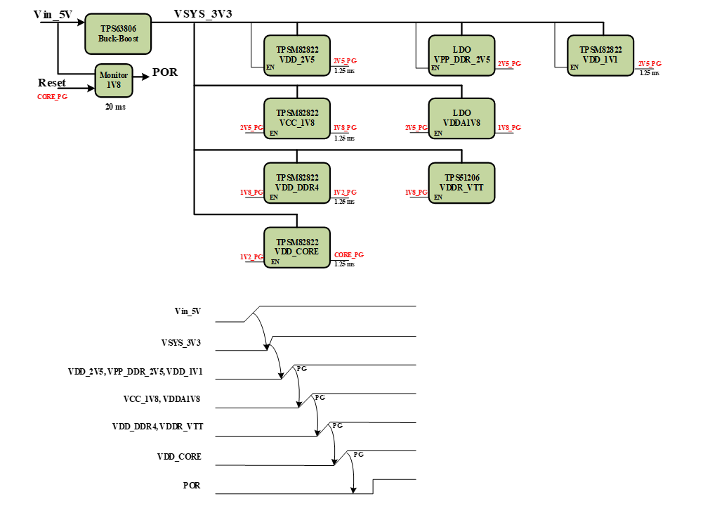
The power architecture main features are:
· Single 5V power source.
· Buck-Boost on the input enable lower power connection e.g. battery.
· 3.3V output up to 1A (Need to calculate system and SOM power).
VPP_1V8
To program the CPU a power of 1.8V is required. To program the CPU, connect a 1.8V to J9-28. For normal operation leave this pin floating.
Reset
The AM64xx power is monitored by a voltage supervisor.
A reset can be triggered by an external reset signal (Switch) or the internal power fail. There is a pull-up on the SOM.
Integration Manual
Power Up Sequence
The AM64xx is sourced by a single 5V input. All power sequences are supported by the PMIC.
When using the SOM 3.3V output there is no need to consider its power sequence. If an external power source is used, it needs to be power according to the power sequence rules. (See AM64xx datasheet for details)
Booting Options
Fuses Booting
Not Supported.
Booting from Resistors setting
The AM64xx SOM can boot from different NVM according to an external resistors configuration.
The available booting NVM are:
· eMMC on MMC0.
· uSD card on MMC1.
· QSPI on QSPIA.
· UART
· USB
| Warning |
|---|
Note – Ethernet boot is NOT supported |
There are 16 boot mode signals [BOOTMODE 0-15]. The table below describes the supported boot option in the AM64xx system (SOM and Carrier).
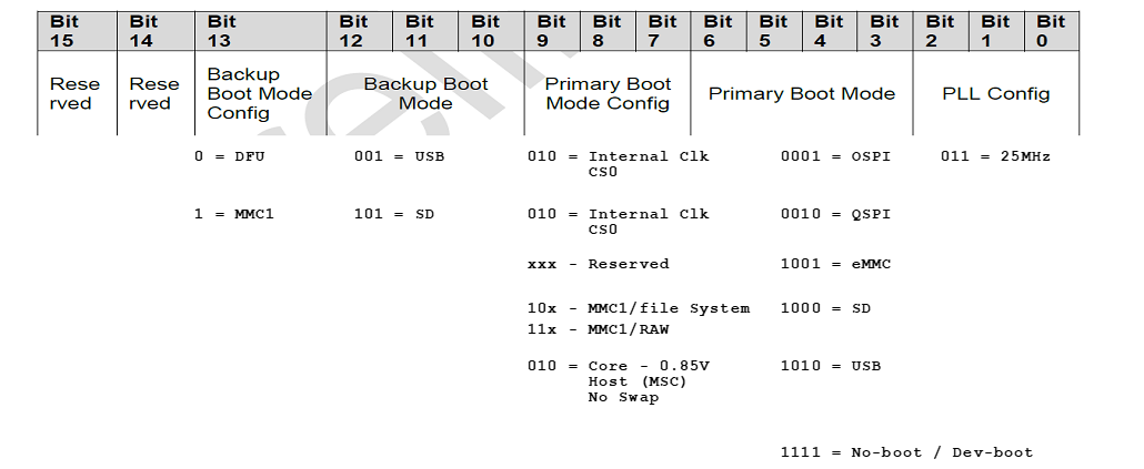
| Note |
|---|
Note – the PLL frequency is set on the SOM. Other frequencies required a special SKU. Note – The Boot signals have an alternative functionality. Make sure it fixed during reset. |
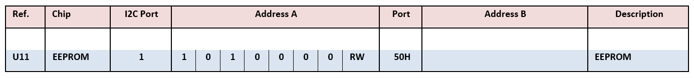
I2C Interfaces
The AM64xx SOM uses I2C0 interface for its internal configurations. The following table describes the address mapping.
GPIO Interfaces
The AM64XX SoC uses some GPIO signals for its internal controls. The following table describes the GPIO allocation.
Signal | I/O | Description | Remarks |
|---|---|---|---|
PRG1_RGMII_INTn | EXTINTn | Ethernet PHYs interrupt | Active Low |
GPIO_CPSW1_RST | GPIO0_84 | Reset Ethernet CPSW1 | Active Low |
GPIO_RGMII1_RST | GPIO0_52 | Reset Ethernet ICSSG1 - RGMII 1 | Active Low |
GPIO_RGMII2_RST | GPIO0_20 | Reset Ethernet ICSSG1 - RGMII 2 | Active Low |
AM64xx Debugging Capability
The AM64XX SOM supports UART interface for debugging.
The UART interface is a null modem interface that is internally pulled up and support using SOC_MAIN_UART0_TX/RX signals.
he UART interface is optional to use and mentioned here since most of the software infrastructure used in HummingBoard Pulse uses it for debugging.
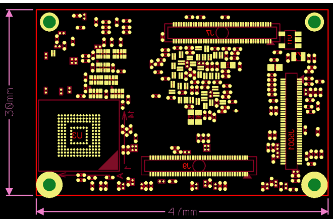
Mechanical Description
Following is a diagram of the TOP and BOTTOM view of the SR-AM64xx.
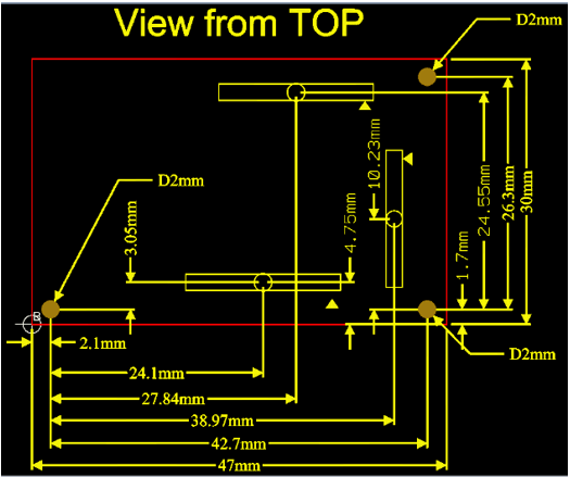
Note the following details:
· The carrier board must use the same footprint as in the above mechanical footprint.
Since this is a TOP VIEW of the print side of the AM64xx, the diagram above describes the dimensions and placement of the board-to-board headers, mechanical holes and boundaries of the AM64xx, as-is.
· J9 is the main board-to-board header (bottom side in the diagram).
· J7 is the second board-to-board header (upper side in the diagram).
· J5001 is the third board-to-board header (right side in the diagram).
· In case 1.5mm mating height was chosen, then the AM64xx requirement would be that all area beneath it on the carrier will be all dedicated ONLY for the board-to-board connectivity; no other components are allowed.
In case higher mating is chosen, then 1.5mm should be reserved for the AM64xx. For instance, if 3.5mm mating height is chosen, then 1.5mm is dedicated to the AM64xx print side components and the remaining 2mm for the carrier components underneath the AM64xx.
Refer to SolidRun HummingBoard design and layout, where there are examples of the main and second 80 pin header board-to-board usage.
Documentation
| Attachments | ||||
|---|---|---|---|---|
|
| Ui button | ||||||
|---|---|---|---|---|---|---|
|
Related Articles
| Filter by label (Content by label) | ||||
|---|---|---|---|---|
|